Low-Voltage Surface-Sensitive Modes in Scanning Electron Microscopy
The scanning electron microscope has been a cornerstone of materials science, biology, and nanotechnology for over half a century. Its ability to form high-resolution images of surfaces by scanning a focused electron beam and detecting the resulting signals is unparalleled. Throughout my career, I have witnessed the evolution of these instruments, from the early days of thermionic emission and kilovolt-range accelerating potentials to the modern era of field emission guns and sophisticated beam deceleration techniques. Among the most significant developments has been the refinement of low-voltage operation, a mode that prioritizes surface sensitivity over ultimate resolution, and which places unique and stringent demands on the high-voltage power supplies that control the electron optics.
The fundamental trade-off in scanning electron microscopy is between resolution and surface sensitivity. A higher accelerating voltage, typically 10 to 30 kilovolts, produces a shorter electron wavelength and allows for a smaller, more focused probe, yielding higher resolution. However, these high-energy electrons penetrate deeply into the sample, interacting with a large interaction volume. The signals that escape, whether secondary electrons, backscattered electrons, or X-rays, originate from a volume that may be many micrometers deep and wide. This obscures fine surface details and can lead to charging artifacts on insulating samples. Low-voltage operation, typically below 5 kilovolts and often down to a few hundred volts or even less, dramatically reduces the interaction volume. The electrons penetrate only tens of nanometers, making the technique exquisitely sensitive to the very surface of the material. This is invaluable for imaging thin films, surface contaminants, delicate biological structures, and for minimizing damage to beam-sensitive specimens.
The challenge of low-voltage operation lies in the electron optics. At low energies, the electrons are highly susceptible to stray electromagnetic fields and to the Coulomb repulsion known as the Boersch effect, which broadens the energy spread of the beam. Furthermore, the objective lens, which focuses the beam onto the sample, typically has aberrations that increase dramatically at low voltages. To overcome these limitations, modern instruments employ a variety of techniques, all of which rely on precise and stable high-voltage control.
One common technique is beam deceleration, or the use of a retarding field. In this mode, the electron gun and the upper column are operated at a relatively high voltage, perhaps 5 to 10 kilovolts, where the optics perform well and the beam can be finely focused. Just before the sample, however, the beam is decelerated by applying a negative bias to the sample itself, or to a stage surrounding it. The final landing energy of the electrons is the difference between the gun voltage and this bias voltage. For example, with a gun at 5 kilovolts and a sample bias of minus 4.5 kilovolts, the landing energy is only 500 electronvolts. This deceleration scheme preserves the high-brightness, low-aberration performance of the high-voltage column while achieving the surface sensitivity of a low-voltage beam.
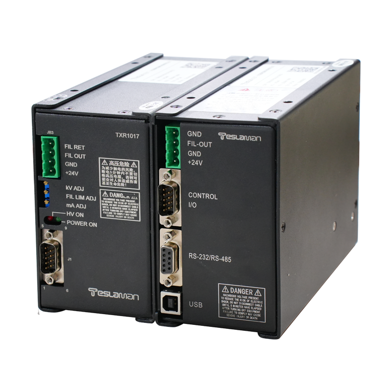
The power supply for the sample bias in such a system is a critical component. It must provide a stable, low-noise voltage, often up to several kilovolts, with the sample and its stage floating at this potential. Any ripple or drift on this bias voltage directly translates into a variation in the landing energy of the electrons, degrading the image resolution and contrast. Furthermore, the bias supply must be able to handle the current from the beam, which, although small, can be significant if the sample is not perfectly conductive. The supply must also incorporate fast-acting protection circuits to shut down the bias in the event of a sample discharge or an arc, protecting both the sample and the sensitive electronics of the microscope.
Another approach to low-voltage operation involves the use of a monochromator. The energy spread of the electron beam, even from a field emission source, is a fundamental limit to the performance of the optics, especially at low voltages where chromatic aberration dominates. A monochromator selects a narrow slice of the energy distribution, reducing the energy spread from perhaps 0.3 electronvolts to below 0.1 electronvolts. This significantly improves the resolution at low landing energies. The monochromator itself is an electrostatic or magnetic device that requires its own set of highly stable, low-noise power supplies. The voltages on the monochromator electrodes must be controlled with parts-per-million precision to maintain the energy selection and to avoid introducing beam drift.
In my laboratory, we have spent years optimizing low-voltage imaging conditions for a variety of materials. For example, in studying the early stages of graphene growth on copper, we needed to image the atomically thin layers with high contrast. Using a beam deceleration setup with a sample bias of several kilovolts, we could achieve landing energies below 100 electronvolts. At these energies, the contrast between a single layer of graphene and the underlying copper substrate was dramatically enhanced. The high-voltage bias supply had to be exceptionally stable, as any fluctuation would cause the image to shift or defocus. We ultimately designed a custom supply with multiple stages of filtering and a low-noise linear regulator, achieving ripple levels below 10 millivolts at a bias of 4 kilovolts.
The evolution of scanning electron microscopy towards ever-lower landing energies is a testament to the ingenuity of electron opticians and the precision of modern high-voltage engineering. The power supplies that provide the accelerating potentials, the lens voltages, and the sample biases are no longer simple accessories; they are integral to the performance of the instrument, enabling us to see the nanoworld with ever-greater clarity and surface sensitivity. The quiet hum of these high-voltage modules, hidden within the microscope column, is the sound of electrons being tamed and shaped into a probe that reveals the secrets of the surface.