Focused Ion Beam Circuit Modification High-Voltage Precision Processing Technology
Focused ion beam technology has revolutionized circuit modification and prototyping in semiconductor industry and research applications.The ability to precisely remove and deposit material at micron and sub-micron scales enables circuit editing,prototype development,and failure analysis.High-voltage precision processing provides enhanced capabilities for demanding circuit modification tasks.
Focused ion beam systems operate by accelerating ion species,typically gallium,to high energies and focusing them to a small spot on the target surface.The kinetic energy of ions causes sputtering,removing material from the target area. By scanning the beam across the surface,precise patterns can be milled with dimensional control on the scale of tens of nanometers.
Circuit modification applications require extremely precise material removal without damaging adjacent structures.Signal routing changes can be implemented by cutting existing conductors and depositing new connections.Probe points can be milled to access internal nodes for debugging.Protection structures can be removed to expose hidden features.
High-voltage operation in focused ion beam systems offers several advantages for precision processing.Higher acceleration voltages produce ions with greater kinetic energy,increasing sputtering yield for faster material removal.The smaller beam spot size achievable at higher voltages improves pattern resolution.Reduced beam divergence improves depth of focus for three-dimensional processing.
However,high-voltage operation also introduces challenges that must be addressed.Gallium implantation at high energy can cause significant damage to sensitive semiconductor devices.High beam energies can cause deeper penetration and larger interaction volumes,reducing precision.Lower beam currents at very high voltages can extend processing times.
The implementation of high-voltage precision processing requires sophisticated control systems.Advanced pattern generation software converts design intent into beam scanning commands.Real-time endpoint detection identifies when processing has reached desired depth or endpoint.Microscope vision systems provide alignment and navigation capabilities.
Material deposition capabilities complement ion beam milling in circuit modification applications.Gas injection systems introduce precursor materials that decompose under ion beam irradiation,depositing material precisely where needed.Conductors,insulators,and semiconductors can all be deposited for different modification requirements.
In semiconductor failure analysis and circuit editing applications,precision processing enables valuable capabilities.Engineering change orders can be implemented without redesigning entire chips.Debugging of prototype circuits becomes possible through strategic cuts and jumps.Failure analysis can isolate defects through precise sectioning.
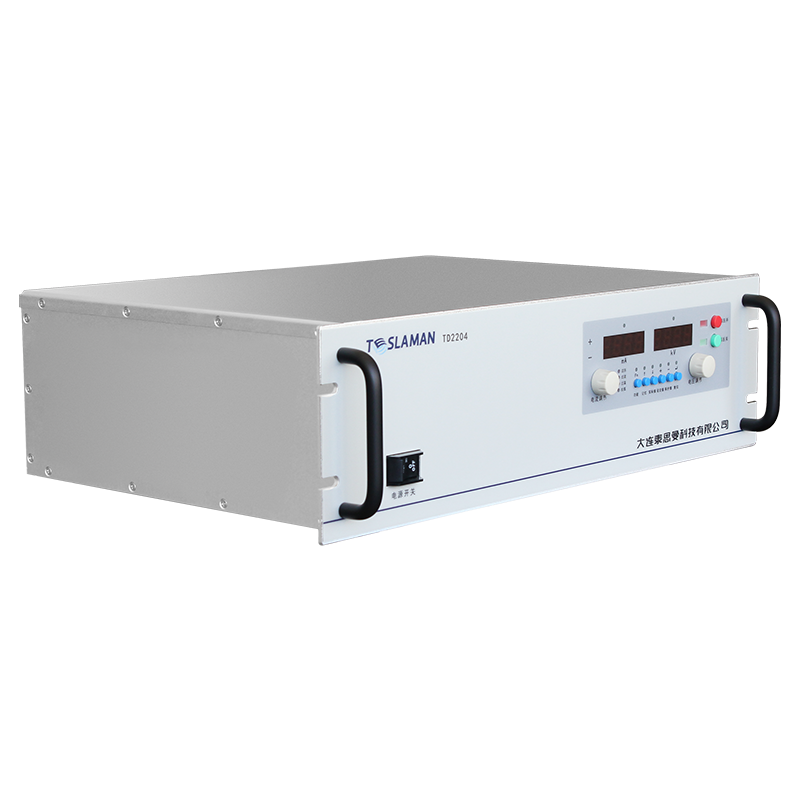
The high-voltage power supplies for focused ion beam systems must provide extremely stable output for consistent processing performance.Voltage stability directly affects beam energy and consequently sputtering yield and resolution.Ripple and noise on the high-voltage supply can degrade beam quality.
Safety considerations in focused ion beam systems require appropriate attention.High voltages present electrical hazards that necessitate comprehensive interlock systems.Gallium is a toxic heavy metal requiring careful handling and disposal.Energetic ions and secondary electrons create radiation considerations.
Economic considerations in focused ion beam circuit modification involve balancing capability against cost and throughput.Equipment investment for high-precision systems is substantial,requiring justification through application value.Modification versus redesign decisions depend on specific circumstances.
Future developments in focused ion beam circuit modification will likely incorporate new ion sources and processing approaches.Liquid metal alloy ion sources offer improved performance for certain applications.Atomically precise processing approaches seek to achieve single-atom control for ultimate precision.
In summary,focused ion beam circuit modification using high-voltage precision processing technology provides powerful capabilities for semiconductor circuit editing and analysis.Through continuous advancement of hardware and process technologies,these systems enable increasingly sophisticated circuit modifications to meet evolving requirements.