RF Shielding Technology of High Voltage Power Supply for Inductively Coupled Plasma Mass Spectrometer
Inductively coupled plasma mass spectrometry is a powerful analytical technique for trace element analysis. The inductively coupled plasma is generated and sustained by radio frequency power applied to an induction coil. The high voltage power supply that biases the interface region must operate in close proximity to the RF field without being affected by electromagnetic interference. RF shielding technology protects the high voltage power supply from the intense RF environment while maintaining electrical performance. Understanding RF shielding principles is essential for reliable ICP-MS operation.
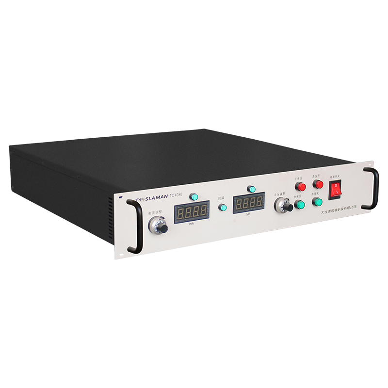
The electrical requirements for ICP-MS high voltage power supplies depend on the instrument design and analytical requirements. The interface voltage typically ranges from hundreds to thousands of volts. The current is typically in the microampere to milliampere range. The power supply must provide stable output despite the intense RF environment. The RF power to the plasma can be hundreds to thousands of watts at frequencies typically around 27 or 40 megahertz.
ICP-MS operation fundamentals involve plasma generation and ion extraction. The RF power applied to the induction coil creates a high-temperature plasma that atomizes and ionizes the sample. The ions are extracted through the interface region into the mass spectrometer. The high voltage on the interface electrodes controls the ion extraction and focusing. Any interference with the high voltage affects the analytical performance.
RF interference mechanisms include direct coupling and ground loops. Direct coupling occurs when RF energy is picked up by the power supply circuits or cables. Ground loops occur when RF currents flow through ground connections. Both mechanisms can cause noise on the high voltage output. The interference can affect the ion extraction and degrade analytical performance.
Shielding principles involve creating barriers to electromagnetic fields. Conductive enclosures reflect and absorb electromagnetic energy. The shielding effectiveness depends on the material conductivity, thickness, and the frequency of the interference. For RF frequencies, even thin conductive materials can provide effective shielding. The key is to create a continuous conductive barrier around the sensitive circuits.
Enclosure design for RF shielding requires attention to seams and openings. Any gap in the shielding can allow RF energy to penetrate. Overlapping seams provide better shielding than butt joints. Conductive gaskets ensure electrical continuity across seams. Openings for cables and ventilation require filtering or waveguide-beyond-cutoff structures. The enclosure must provide complete shielding coverage.
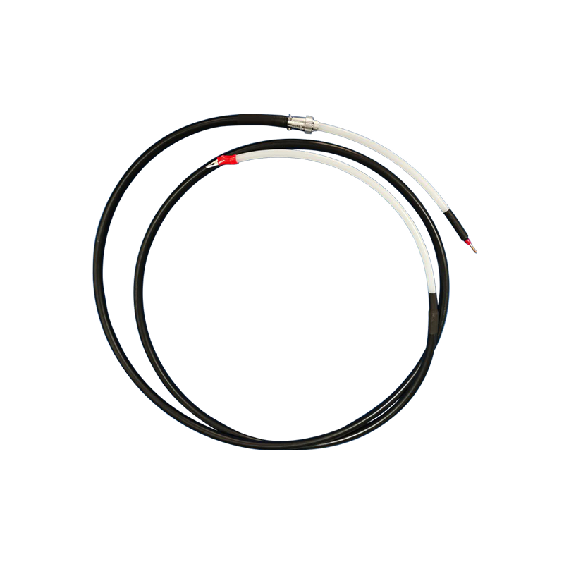
Cable shielding prevents RF pickup on interconnecting cables. Shielded cables have a conductive braid or foil surrounding the signal conductors. The shield must be properly terminated at both ends to provide effective shielding. Pigtail connections can compromise shielding effectiveness. The cable shielding must be compatible with the enclosure shielding to provide complete protection.
Filtering prevents RF from entering through power and signal lines. Power line filters attenuate RF on the input power. Signal line filters protect control and monitoring circuits. The filter cutoff frequency must be below the RF frequency to provide adequate attenuation. The filters must be properly installed with short connections to the shielded enclosure.
Grounding design affects RF immunity. A single-point ground prevents ground loops. The ground connection should be made at a single point to avoid multiple paths for RF currents. The ground impedance must be low at RF frequencies. Wide conductors or ground planes provide low impedance. The grounding design must be coordinated with the shielding design.
Component selection for RF immunity includes choosing components with low RF susceptibility. Linear regulators are generally more immune than switching regulators. Analog circuits can be protected with filtering and shielding. Digital circuits may require special attention to clock frequencies that could interfere with the RF. The component placement should minimize the loop area of sensitive circuits.
PCB layout affects RF susceptibility. Ground planes provide shielding and low-impedance return paths. Proper layer stackup separates sensitive circuits from potential interference sources. Trace routing should minimize loop areas. Decoupling capacitors should be placed close to integrated circuits. The PCB design should follow good EMC practices.
Testing and validation of RF immunity verify the shielding effectiveness. The power supply can be tested in an RF field to simulate the ICP environment. The output noise and stability are measured under RF exposure. The shielding effectiveness can be measured using standard methods. The testing should cover the expected RF power levels and frequencies.
Installation considerations affect the RF immunity in practice. The power supply location relative to the RF coil affects the interference level. Cable routing should avoid proximity to the RF coil. Grounding connections should follow the designed scheme. The installation should maintain the shielding integrity.
Applications of ICP-MS include environmental analysis, geological exploration, and clinical diagnostics. Each application has specific requirements for sensitivity and stability. The RF shielding design must support the analytical performance requirements.