Dynamic Voltage Control Study of Electrostatic Chuck High Voltage Power Supply in Wafer Bonding Process
Wafer bonding has become an essential process in semiconductor manufacturing, enabling the creation of three-dimensional integrated circuits, microelectromechanical systems, and advanced packaging structures. The electrostatic chuck holds the wafer during bonding operations using electrostatic attraction forces generated by high voltage. The dynamic voltage control of the electrostatic chuck power supply significantly affects the bonding quality, process throughput, and wafer integrity.
Electrostatic chucks operate on the principle of electrostatic attraction between charged electrodes and the wafer. When a high voltage is applied to electrodes embedded in the chuck surface, an electric field is established between the electrodes and the wafer. The resulting electrostatic force attracts the wafer to the chuck surface, providing mechanical stability during processing. The holding force depends on the applied voltage, the electrode geometry, and the dielectric properties of the intervening materials.
Wafer bonding processes require precise control of temperature, pressure, and alignment. The electrostatic chuck must maintain stable wafer position throughout the bonding cycle, which may involve temperature changes of hundreds of degrees and applied pressures of several megapascals. The chucking force must be sufficient to prevent wafer movement but not so high as to cause damage when the wafer is released.
Dynamic voltage control refers to the ability to adjust the chucking voltage in real time during the bonding process. The optimal chucking voltage varies with the process conditions. At room temperature, a certain voltage provides adequate holding force. As the temperature increases during bonding, the dielectric properties of the materials change, affecting the chucking force. The voltage must be adjusted to maintain consistent holding force throughout the temperature cycle.
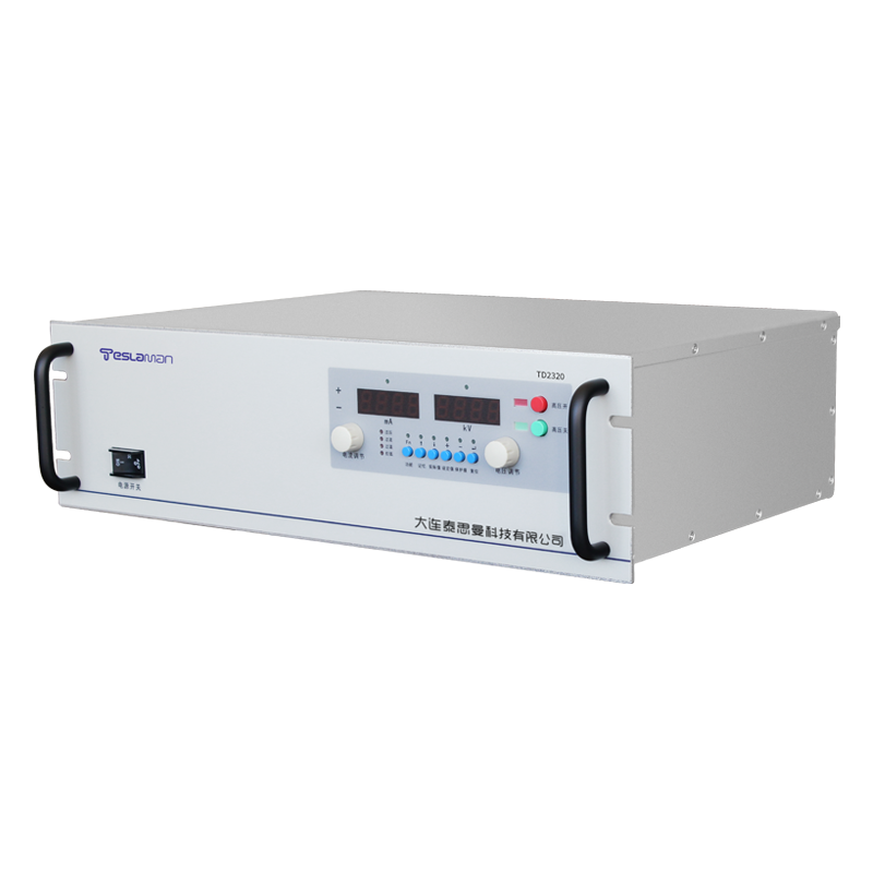
The high voltage power supply for electrostatic chucks typically operates in the range of several hundred to several thousand volts. The supply must provide precise voltage control with fast response to commanded changes. The output current is typically small, measured in microamperes or milliamperes, as the chuck behaves primarily as a capacitive load. However, the supply must be capable of supplying sufficient current during voltage transitions to charge the chuck capacitance quickly.
Voltage ripple affects the chucking force stability. The electrostatic force is proportional to the square of the voltage, so voltage variations cause force variations. Excessive ripple can cause micro-movements of the wafer, potentially affecting alignment or bonding quality. The power supply must provide clean DC output with minimal ripple, typically specified as a small fraction of the output voltage.
The dynamic response of the power supply is critical for process control. When the process recipe calls for a voltage change, the supply must execute the change quickly and accurately. Slow response limits the process throughput and may cause process timing issues. Overshoot or undershoot during transitions can cause temporary force variations that affect the wafer position.
Digital control enables sophisticated voltage profiles during the bonding cycle. The voltage can be programmed to follow complex trajectories synchronized with temperature and pressure profiles. This flexibility enables optimization of the chucking force for each phase of the bonding process. Modern power supplies often include programmable waveform generators that can store and execute voltage profiles without real-time communication with the process controller.
Safety considerations are paramount when operating high voltage near valuable wafers. The power supply must include protection against overvoltage, overcurrent, and arc detection. An arc between the chuck electrode and the wafer can damage both the wafer and the chuck. Fast arc detection and voltage suppression minimize damage when arcs occur. The power supply should include current limiting and energy limiting features to reduce arc severity.
Wafer release after bonding requires controlled voltage reduction. Simply turning off the high voltage can leave residual charge on the chuck, causing the wafer to stick. A controlled release sequence gradually reduces the voltage while monitoring the wafer position. Some implementations include reverse polarity pulses to neutralize residual charge. The power supply must support these release sequences with appropriate voltage polarity and control.
The interaction between multiple electrostatic chucks in a bonding system adds complexity. In systems with both top and bottom chucks, the voltages must be coordinated to achieve the desired force distribution. Differential voltages between chucks can create lateral forces that affect wafer alignment. The power supplies for multiple chucks must be synchronized and coordinated through the system controller.
Calibration and monitoring of the chucking force enable process optimization and fault detection. The relationship between applied voltage and chucking force depends on the chuck geometry, wafer properties, and environmental conditions. Regular calibration ensures that the voltage control achieves the intended force. Monitoring of the voltage and current during operation can detect anomalies such as partial wafer lift or chuck degradation.