Stress Compensation Algorithm for Zoned High Voltage Power Supply of 12 Inch Wafer Electrostatic Chuck
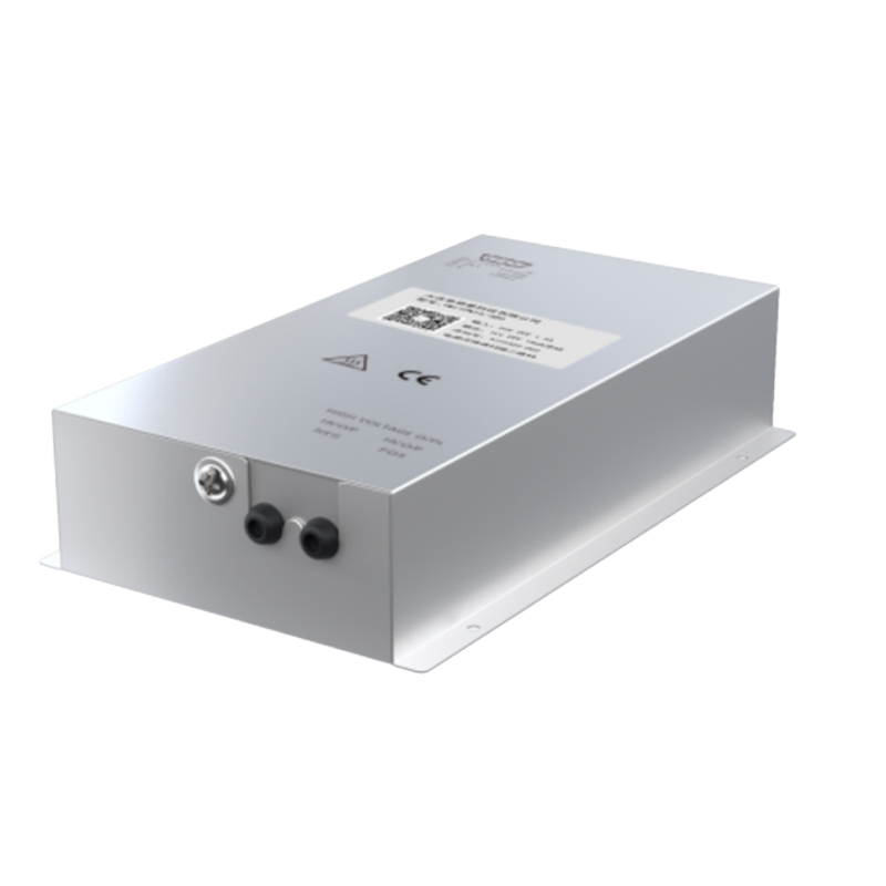
Electrostatic chucks have become essential for holding wafers during semiconductor manufacturing processes. The twelve inch wafer size, the current standard for advanced semiconductor production, presents challenges for achieving uniform chucking force across the entire wafer surface. Zoned electrostatic chucks with independently controlled high voltage supplies to different zones enable compensation for wafer stress and distortion. The stress compensation algorithm optimizes the zone voltages to achieve uniform holding force and minimize wafer distortion.
Electrostatic chucks operate by applying a high voltage to electrodes embedded in the chuck surface. The resulting electric field creates an attractive force between the electrodes and the conductive wafer. The chucking force depends on the applied voltage, the electrode geometry, and the dielectric properties of the chuck surface layer. The force must be sufficient to hold the wafer securely against the chuck during processing.
Wafer stress and distortion arise from several sources. Thermal gradients during processing cause differential expansion that bends the wafer. Film stresses from deposited layers create intrinsic stress in the wafer. Mechanical handling can introduce residual stresses. These stresses cause the wafer to deviate from flatness, creating gaps between the wafer and the chuck in some regions. These gaps affect heat transfer and can cause processing non-uniformity.
Zoned electrostatic chucks divide the chuck surface into multiple independently controlled zones. Each zone has its own electrode structure and high voltage supply. By applying different voltages to different zones, the chucking force can be varied across the wafer. This spatial variation in force can compensate for wafer distortion, pulling the wafer flat against the chuck.
The stress compensation algorithm determines the optimal voltage for each zone to achieve the desired chucking condition. The algorithm requires a model of the relationship between zone voltages and the resulting wafer shape. This model must account for the electrostatic forces, the wafer mechanical properties, and the chuck geometry. The model can be physics based, using finite element analysis, or empirical, based on measured data.
The electrostatic force model calculates the force distribution on the wafer for given zone voltages. The force depends on the electric field, which is determined by the electrode geometry and the dielectric properties. The field is affected by the gap between the wafer and the chuck, creating a coupled problem where the force depends on the gap, and the gap depends on the force through the wafer deformation.
The wafer deformation model calculates the wafer shape resulting from the applied forces. The wafer behaves as a thin elastic plate, and its deformation can be calculated using plate theory or finite element analysis. The deformation depends on the wafer thickness, elastic modulus, and any intrinsic stress in the wafer. The model predicts the gap distribution for given electrostatic forces.
Iterative algorithms solve the coupled electrostatic and mechanical problem. Starting from an initial guess of the zone voltages, the algorithm calculates the forces, then the deformation, then updates the voltages to reduce the gap. The iteration continues until the gap is minimized or the desired chucking condition is achieved. Convergence depends on the algorithm design and the problem characteristics.
Optimization algorithms can directly search for the zone voltages that minimize an objective function. The objective function might include the maximum gap, the average gap, or a weighted combination. Constraints ensure that the voltages remain within safe limits and that the chucking force is sufficient for processing. Various optimization methods including gradient descent, genetic algorithms, and simulated annealing can be applied.
Real time implementation requires efficient algorithms that can compute the zone voltages within the available time. The algorithm may run during process setup to establish the initial chucking condition, or it may run continuously during processing to adapt to changing conditions. Fast execution enables responsive compensation for thermal transients or other time varying effects.
Calibration characterizes the chuck and wafer behavior for accurate compensation. Test measurements using capacitive sensors or optical techniques measure the gap distribution for known zone voltages. These measurements establish the parameters of the compensation model. Regular recalibration accounts for chuck wear, contamination, or other changes that affect the electrostatic characteristics.