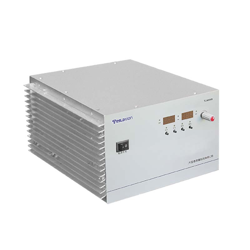
Low Frequency Noise Suppression of Bias High Voltage Power Supply for Superconducting Transition Edge Sensor
Superconducting transition edge sensors represent the state of the art in photon and particle detection, offering simultaneous measurement of energy and arrival time with resolution approaching fundamental limits. These sensors operate at the superconducting transition temperature, where the resistance changes sharply with temperature. A bias voltage or current maintains the sensor in the transition region, with absorbed photons causing temperature excursions that produce resistance changes detectable as current or voltage signals. The noise performance of the bias power supply directly affects the sensor sensitivity, with low frequency noise being particularly problematic as it falls within the signal bandwidth of typical measurements. Effective low frequency noise suppression enables the sensor to achieve its ultimate performance capabilities.
The transition edge sensor exploits the steep resistance versus temperature curve of a superconductor at its critical temperature. When biased in the transition region, small temperature changes produce large resistance changes, providing high sensitivity to energy deposition. The sensor is typically voltage biased using a low noise voltage source in parallel with a shunt resistor, or current biased using a low noise current source. The bias stability determines the operating point stability and the conversion of sensor signals to measurable outputs.
Noise in the bias supply appears directly in the sensor output, degrading the energy and timing resolution. The noise contributions include voltage or current noise from the supply, noise from the bias circuit components, and noise coupled from the environment. The total noise must be below the intrinsic sensor noise to avoid degrading the sensor performance. For the best transition edge sensors, this requires noise levels measured in picovolts per root hertz or picoamperes per root hertz.
Low frequency noise, often characterized as one over f noise or flicker noise, increases at lower frequencies and can dominate the noise budget in the signal bandwidth. This noise arises from various sources including semiconductor defects, dielectric polarization, and thermal fluctuations in components. The low frequency noise is particularly important for transition edge sensors because the signal bandwidth extends to low frequencies for the relatively slow thermal response of the sensors.
Power supply design for low noise begins with the selection of low noise components. Voltage references based on buried zener diodes or junction field effect transistors offer lower noise than switching regulators or standard integrated circuit references. The reference noise sets the fundamental limit for the supply output noise. Low noise operational amplifiers and transistors in the regulation circuits minimize the additional noise contributions.
Filtering reduces noise from the power supply and coupling from external sources. Low pass filters attenuate high frequency noise above the signal bandwidth. Active filters can provide sharper cutoff characteristics and maintain low output impedance in the passband. For low frequency noise, filtering is less effective because the noise falls within the passband where the filter provides little attenuation. The fundamental approach for low frequency noise is to minimize the noise generation rather than relying on filtering.
Battery power provides inherently low noise compared to line powered supplies, as batteries have no switching or rectification noise and no connection to the noisy electrical mains. However, batteries have finite capacity and require replacement or recharging, complicating long duration measurements. Hybrid approaches using batteries for the most sensitive circuits and line power for less critical functions can balance noise performance against operational convenience.
Cryogenic operation of bias circuit components can reduce thermal noise and improve stability. Operating resistors and semiconductors at cryogenic temperatures reduces the thermal noise spectral density proportional to the square root of temperature. Some components may exhibit different noise characteristics at cryogenic temperatures, potentially improving or degrading depending on the noise mechanisms. The bias supply may be located at room temperature with filtered connections to the cryogenic sensor, or may be partially or fully cryogenic for the lowest noise performance.
Feedback regulation can either increase or decrease the output noise depending on the implementation. The feedback loop compares the output with a reference and adjusts the output to minimize the error. Noise in the reference and the error amplifier appears at the output within the loop bandwidth. Outside the loop bandwidth, the output noise reflects the unregulated source noise. The loop design must balance the noise contributions from different sources across the frequency range.
Temperature stability of the bias circuit affects the low frequency noise through temperature dependent drifts that appear as low frequency fluctuations. Component values, reference voltages, and amplifier offsets vary with temperature, causing output variations as the temperature changes. Temperature control of sensitive components or temperature compensation circuits reduce these drifts. The thermal time constants of the system determine how temperature fluctuations at different frequencies translate to output fluctuations.
Grounding and shielding prevent coupling of external noise into the bias circuit. The sensor and bias circuit form a sensitive node that can pick up interference from electromagnetic fields, ground voltage differences, and capacitive or inductive coupling to nearby circuits. Proper grounding topology, with single point connections between subsystem grounds, avoids ground loops that can couple noise. Shielding enclosures attenuate electromagnetic interference. Twisted pair or coaxial cables for bias connections reduce magnetic and electric field coupling.
Measurement of the bias supply noise requires techniques with sensitivity comparable to or better than the noise being measured. Cross correlation techniques using two independent measurement channels can reduce the noise floor below the noise of the individual measurement systems. The sensor itself can serve as a noise monitor, measuring the noise in the output when no signal is present. Comparison of the measured noise with the expected sensor noise indicates whether the bias supply noise is significant.