Thermal Stress Compensation Algorithm for Zoned High Voltage Power Supply of 18 Inch Wafer Electrostatic Chuck
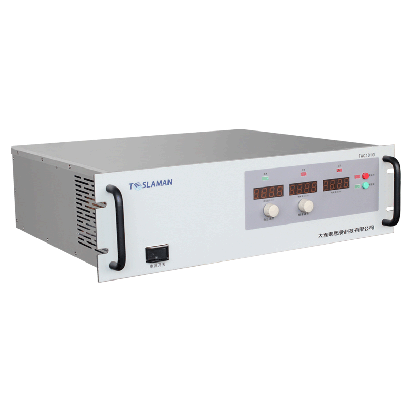
Eighteen inch wafer processing represents the frontier of semiconductor manufacturing scale, demanding increasingly sophisticated wafer handling capabilities. Electrostatic chucks provide the clamping force to hold wafers during plasma etching, chemical vapor deposition, and other high temperature processes. The thermal expansion mismatch between the wafer and the chuck structure creates stress that can cause wafer slip, distortion, or breakage. Zoned electrostatic chucks with independently controlled electrode regions enable spatial variation of the clamping force to compensate for thermal stress distributions. The high voltage power supply driving each zone must implement compensation algorithms that maintain appropriate clamping force as temperature distributions evolve during processing.
The electrostatic chuck operates by applying high voltage to electrodes embedded within a dielectric structure, creating electrostatic attraction between the electrodes and the conductive wafer. The clamping force depends on the applied voltage, the dielectric properties of the chuck material, and the gap between the wafer and the chuck surface. During processing, the wafer and chuck heat nonuniformly due to plasma exposure, backside gas cooling, and heat transfer through the chuck to the cooling system. The resulting temperature distribution causes thermal expansion that varies across the chuck surface.
Thermal stress arises from the differential expansion between the wafer and the chuck, and from the temperature gradients within each component. Silicon wafers have a well defined thermal expansion coefficient, while the chuck dielectric material, typically aluminum nitride or alumina, has a different coefficient. When the wafer expands more than the chuck, tensile stress develops at the interface. When the chuck expands more, compressive stress develops. These stresses can cause the wafer to slip on the chuck surface, distorting the pattern registration, or can cause wafer breakage if the stress exceeds the silicon strength.
Zoned chuck designs divide the electrode structure into multiple independently controlled regions, typically arranged in concentric rings or rectangular zones. Each zone can be powered at a different voltage, creating spatial variation in the clamping force. By increasing the clamping force in regions experiencing high thermal stress, the local friction between wafer and chuck can be increased to resist slip. The compensation algorithm determines the appropriate voltage for each zone based on the measured or predicted temperature distribution.
Temperature measurement provides the input for the compensation algorithm. Thermocouples embedded in the chuck structure measure the local temperature at discrete points. Infrared pyrometry measures the wafer backside temperature, though the measurement is complicated by the chuck structure and any backside gas. Plasma optical emission can provide information about the heat flux to the wafer surface. The temperature data feeds into a thermal model that estimates the temperature distribution across the chuck and wafer.
The thermal model calculates the temperature field from the heat sources, the heat transfer paths, and the thermal boundary conditions. Finite element thermal analysis provides the most accurate prediction but requires significant computation. Reduced order models derived from finite element analysis capture the essential thermal behavior with much faster computation, enabling real time implementation. The model must account for the process dependent heat flux, the cooling system performance, and the thermal contact resistance between wafer and chuck.
Stress calculation from the temperature distribution determines the thermal stress field in the wafer. The stress depends on the temperature relative to a stress free reference temperature, the thermal expansion coefficients, and the mechanical constraints from the clamping force. Regions where the stress exceeds the slip threshold require increased clamping force to prevent wafer movement. The stress model may also predict regions where excessive clamping force could cause wafer damage, requiring voltage reduction.
The compensation algorithm translates the stress distribution into zone voltage commands. The algorithm may use a lookup table relating temperature patterns to voltage settings, a parametric model calculating voltages from temperature values, or an optimization approach that minimizes a cost function combining slip risk and clamping uniformity. The algorithm must execute fast enough to track the thermal transients during process steps, which may have time constants of seconds.
Voltage slew rate limiting prevents rapid changes in clamping force that could excite wafer vibrations or cause sudden slip. The algorithm should ramp the voltages smoothly even if the calculated target voltages change abruptly. The ramp rate depends on the wafer mass, the chuck compliance, and the acceptable wafer motion during the transition.
Process integration requires coordination between the compensation algorithm and the process control system. The algorithm must receive process state information including plasma power, gas flows, and pressure that affect the thermal loading. The algorithm outputs the zone voltages to the high voltage power supply controllers. Communication interfaces and timing synchronization ensure that the compensation responds appropriately to process events.
Calibration of the thermal and stress models ensures accurate compensation. Temperature measurements under known conditions verify the thermal model predictions. Wafer distortion measurements after processing validate the stress model and the compensation effectiveness. The calibration data may vary with wafer type, chuck condition, and process recipe, requiring periodic recalibration or model adaptation.