Dielectric Layer Charge Injection and Dissipation Dynamics Research of Electrostatic Chuck High Voltage Power Supply
Electrostatic chucks have become indispensable components in semiconductor manufacturing equipment, providing secure wafer fixation without mechanical clamping that could introduce contamination or damage. The fundamental operating principle involves applying high voltage to electrodes embedded within a dielectric layer, generating electrostatic forces that hold the wafer against the chuck surface. Understanding the charge injection and dissipation dynamics within the dielectric layer is essential for optimizing chuck performance and ensuring reliable wafer handling throughout the manufacturing process.
The dielectric layer in electrostatic chucks serves dual functions of electrical insulation and force transmission. Typical dielectric materials include polyimide, ceramic, or specialized polymer composites selected for their electrical properties, thermal stability, and mechanical durability. When high voltage is applied, the electric field within the dielectric causes charge injection at the electrode-dielectric interface, initiating a complex dynamic process that determines the chucking force and response characteristics.
Charge injection mechanisms at the electrode-dielectric interface depend on several factors including the electrode material, dielectric surface condition, applied voltage magnitude, and temperature. Schottky emission and Fowler-Nordheim tunneling represent the primary injection mechanisms, with the dominant process depending on the electric field strength and interface barrier characteristics. Understanding these mechanisms enables prediction of injection rates and optimization of interface design for desired chuck performance.
The injected charges migrate through the dielectric layer under the influence of the applied electric field, creating a space charge distribution that modifies the internal field profile. This space charge limited conduction results in non-uniform field distributions that differ significantly from the simple capacitive field pattern assumed in ideal dielectric models. The time-dependent evolution of the space charge distribution determines the chucking force dynamics during the initial chucking phase.
Dissipation dynamics govern the release of stored charge when the high voltage is removed, directly impacting wafer release characteristics. Charge trapped in deep energy states within the dielectric bandgap may persist for extended periods, causing residual chucking force that impedes wafer release. The dissipation rate depends on trap energy distribution, temperature, and the presence of detrapping mechanisms such as thermal excitation or optical stimulation.
Temperature effects on charge injection and dissipation dynamics are particularly significant in semiconductor manufacturing applications where process temperatures may range from room temperature to several hundred degrees Celsius. Higher temperatures generally increase charge injection rates due to enhanced carrier mobility and reduced interface barriers. However, elevated temperatures also accelerate charge dissipation through increased thermal excitation of trapped carriers. This temperature dependence requires careful consideration in chuck design for high-temperature processes.
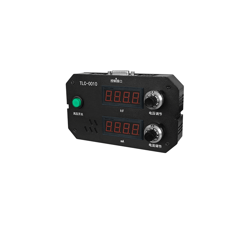
The high voltage power supply characteristics significantly influence charge injection and dissipation behavior. Voltage rise time during chucking affects the initial charge injection dynamics, with faster rise times potentially causing transient overshoot in chucking force. The steady-state voltage level determines the equilibrium charge distribution and chucking force magnitude. Power supply noise and ripple can modulate the charge injection rate, potentially causing chucking force variations that affect process uniformity.
Current limiting in the high voltage power supply serves dual purposes of protecting the chuck electrodes and controlling the charge injection rate. Excessive current can cause localized heating or dielectric breakdown at the electrode interface. Current-limited power supplies ensure that charge injection proceeds at a controlled rate, enabling predictable chucking force development and preventing damage to the chuck or wafer.
The voltage waveform applied during the chucking cycle can be optimized to enhance performance characteristics. Multi-step voltage application with intermediate hold periods allows charge distribution to stabilize before full voltage is applied, reducing transient overshoot. Ramp profiles with controlled rise times enable smoother charge injection dynamics. These advanced waveforms require power supplies with programmable output capability and precise timing control.
Dechucking sequences must be carefully designed to ensure complete wafer release without damage. Simple voltage removal may leave residual trapped charge that maintains partial chucking force. Reverse polarity voltage application can actively extract trapped charge, accelerating the release process. The optimal dechucking waveform depends on the dielectric material properties and the specific charge trapping characteristics of the chuck design.
Charge monitoring during the chucking process provides valuable information about chuck condition and process quality. The current flowing into the chuck electrodes during voltage application reflects the charge injection rate. Analysis of this current waveform can identify anomalies such as dielectric degradation, contamination, or wafer backside defects. Power supplies with integrated current monitoring enable real-time process diagnostics.
Long-term charge accumulation effects can degrade electrostatic chuck performance over time. Repeated chucking cycles may cause gradual buildup of trapped charge in deep energy states that does not fully dissipate during normal dechucking sequences. This accumulated charge can cause chucking force drift, reduced chucking uniformity, or incomplete wafer release. Periodic conditioning cycles with extended reverse polarity voltage application can restore chuck performance by removing accumulated charge.
Dielectric material selection significantly impacts charge injection and dissipation characteristics. Materials with higher dielectric constants enable stronger chucking forces at lower voltages but may exhibit different charge trapping behavior. Materials with wider bandgaps generally exhibit lower charge injection rates but may also have slower dissipation dynamics. Composite materials with optimized filler particles can provide tailored electrical and thermal properties for specific applications.
Interface engineering between the electrode and dielectric layers can modify charge injection characteristics. Thin interfacial layers with controlled properties can reduce injection rates or modify the energy distribution of injected carriers. Surface treatments of the dielectric layer can alter trap densities and energy distributions, affecting both injection and dissipation dynamics. These interface modifications require careful characterization to ensure long-term stability.
Modeling of charge injection and dissipation dynamics enables predictive design of electrostatic chucks. Numerical simulations incorporating charge transport models, trap kinetics, and field-dependent mobility can predict chucking force evolution under various operating conditions. These models require accurate material parameters obtained through experimental characterization, creating a tight coupling between modeling and measurement efforts.
Experimental characterization of charge dynamics typically employs techniques such as thermally stimulated current measurements, isothermal transient current analysis, and surface potential mapping. These methods provide information about trap energy distributions, carrier mobilities, and charge distribution profiles within the dielectric layer. Correlation of these measurements with chuck performance enables refinement of material models and design optimization.
The high voltage power supply must provide stable, well-controlled output for accurate characterization of charge dynamics. Low noise and ripple are essential for distinguishing genuine material response from power supply artifacts. Precise voltage control enables measurement of injection and dissipation rates as functions of applied field. Programmable waveforms facilitate advanced characterization techniques such as double injection and deep level transient spectroscopy.
Reliability considerations for electrostatic chuck power supplies include protection against overvoltage and overcurrent conditions that could damage the chuck or wafer. Arc detection circuits identify dielectric breakdown events and rapidly remove voltage to prevent damage. Soft start circuits limit inrush current during initial voltage application, protecting both the power supply and chuck. These protection functions must operate reliably over millions of chucking cycles typical of semiconductor manufacturing equipment.
Continued advancement in semiconductor manufacturing technology drives ongoing research into dielectric layer charge dynamics. Smaller feature sizes, new materials, and more demanding process requirements create ever more stringent chuck performance specifications. Understanding and controlling charge injection and dissipation dynamics remains essential for meeting these evolving requirements and enabling next-generation semiconductor manufacturing capabilities.