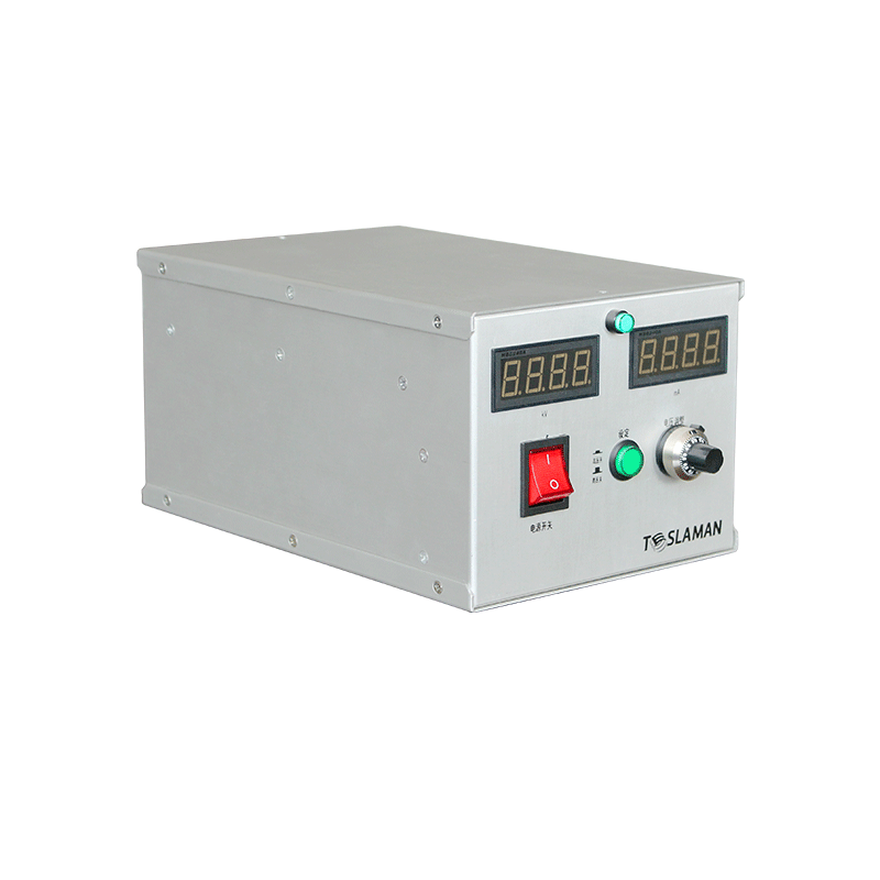
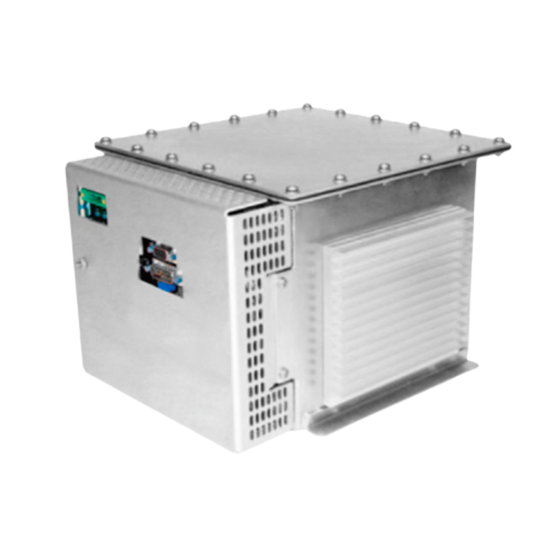
E-CHUCK High Voltage Power Supply Polarity Switching Stability Study in Wafer Fixing
Electrostatic chucks in semiconductor manufacturing processes may require polarity switching capability to accommodate different wafer types, process conditions, or operational sequences. Bipolar electrostatic chucks can operate with either positive or negative clamping voltage, enabling optimization for different substrate materials and process requirements. Stability during polarity switching transitions directly affects wafer handling reliability and process continuity, requiring careful study of the transient phenomena and power supply response characteristics that determine switching performance.
Polarity switching in electrostatic chuck applications serves several operational purposes. Different wafer materials may have different optimal clamping polarities based on the charge transport mechanisms in the wafer-chuck interface. Some processes require alternating polarity for charge neutralization or to prevent electrostatic charge accumulation on the wafer. Wafer handling sequences may use polarity changes to facilitate dechucking after processing. The ability to switch polarity during operation adds flexibility to process development and enables optimization for diverse manufacturing requirements. Understanding the stability characteristics during switching ensures that this capability enhances rather than compromises manufacturing reliability.
The physical mechanisms of electrostatic clamping differ between polarities due to the asymmetric nature of charge transport in semiconductor materials. Positive clamping voltage attracts electrons in the wafer toward the chuck surface, creating the electrostatic attraction force. Negative voltage attracts holes or positive charge carriers. The mobility and availability of these carriers differ, causing different clamping characteristics for the two polarities. The force-voltage relationship may not be symmetric between polarities, requiring separate calibration for each. Process requirements may specify preferred polarity based on substrate doping type, resistivity, and surface condition. Polarity-dependent performance characterization enables appropriate polarity selection for different wafers.
Transition dynamics during polarity switching involve complex electrical and mechanical phenomena. The chuck capacitance must be discharged from one polarity and charged to the opposite polarity, requiring substantial current flow during the transition. The rate of voltage change affects the stress on dielectric materials and the transient forces on the wafer. Rapid switching minimizes transition time but may cause mechanical transients that affect wafer position. Slow switching provides gentler transitions but extends the time when clamping force is uncertain. The optimal switching profile depends on the specific chuck design and wafer handling requirements. Switching profile optimization must balance transition time against stability requirements.
Residual charge effects complicate polarity switching stability. After operating at one polarity, charge may remain trapped in the chuck dielectric or at interfaces even after the voltage is removed. This residual charge creates a clamping force component that persists during the polarity transition. When the opposite polarity is applied, the residual charge may interact with the new applied charge, creating transient forces different from steady-state clamping characteristics. The residual charge decays over time with a time constant determined by dielectric properties. Understanding residual charge behavior enables prediction of actual clamping force during transitions and design of appropriate switching sequences.
Arcing during polarity transitions represents a potential failure mode that must be prevented. The voltage across the chuck dielectric during a polarity reversal can briefly exceed the steady-state voltage by the amount of residual charge present. If this transient voltage exceeds the dielectric strength, arcing can occur, potentially damaging the chuck and wafer. The power supply current limiting must constrain the rate of voltage change to prevent excessive transient voltages. Voltage monitoring during transitions must have sufficient bandwidth to capture transient peaks. Arc detection circuits must distinguish normal switching transients from genuine fault conditions. Arc prevention through controlled switching profiles improves chuck reliability.
Charge neutralization sequences during polarity switching can improve wafer release characteristics. By briefly applying voltage of opposite polarity before dechucking, trapped charge in the wafer-chuck interface can be neutralized, reducing sticking forces. The duration and amplitude of neutralization must be optimized for specific chuck and wafer combinations. Incomplete neutralization leaves residual sticking, while excessive neutralization can cause over-discharge and potential wafer damage. Neutralization sequences may also be applied during wafer handling to prevent static charge buildup on the wafer. Process integration of neutralization sequences must account for timing constraints in wafer handling operations.
Thermal effects during polarity switching arise from power dissipation in the chuck dielectric and resistive layers. Each switching cycle dissipates energy as the chuck capacitance is charged and discharged. At high switching frequencies or high voltages, this energy can cause temperature rise in the chuck. Temperature changes affect dielectric properties and thus clamping characteristics. The power supply must limit switching frequency or provide adequate cooling to maintain temperature stability. Thermal modeling of the chuck during switching operation enables prediction of temperature evolution and design of appropriate thermal management.
Multi-zone chuck configurations require coordinated polarity switching across zones. Each zone may require separate voltage control with appropriate timing relationships during switching. Simultaneous switching of all zones provides symmetric transitions but may require higher peak current capability from the power supply. Sequenced switching reduces peak current but extends overall transition time. Zone interactions through shared substrates or mechanical connections may affect switching dynamics. Zone coordination algorithms must account for these interactions to achieve stable transitions across the entire chuck surface. Zone switching characterization must verify stable operation for all expected switching sequences.
Process environment effects on polarity switching stability include plasma conditions, temperature, and vacuum level. Plasma exposure during processing can charge the chuck surface and modify the charge state at switching initiation. Temperature variations affect dielectric properties and thus switching characteristics. Vacuum level affects charge transport and potential for arcing. The power supply switching parameters may need adjustment for different process conditions to maintain stable operation. Environmental compensation algorithms can adjust switching profiles based on measured conditions. Process-specific switching parameter libraries enable optimization for different process recipes.
Monitoring and diagnostics during polarity switching enable detection of developing problems and provide data for process optimization. Voltage and current waveforms during switching transitions reveal chuck condition and proper operation. Deviations from baseline waveforms may indicate dielectric degradation, contamination, or other problems. Trend analysis of switching waveforms over time supports predictive maintenance. Integration of switching diagnostics into process control systems enables automated response to detected anomalies. Diagnostic data logging provides documentation for quality management systems.
Safety considerations during polarity switching address both electrical hazards and mechanical hazards from wafer movement. The high voltage applied during switching poses electrical shock hazards requiring appropriate enclosure and interlocking. Rapid voltage changes can generate electromagnetic interference that must be controlled. Mechanical transients during switching could potentially dislodge wafers if switching parameters are inappropriate. Safety interlocks must prevent switching under conditions that could cause hazards. Safety system design must account for the specific risks of polarity switching operation. Testing must verify safe operation under all expected switching conditions including fault conditions.