E-CHUCK High Voltage Power Supply Adaptability Research in Next-Generation Wafer Processing
Electrostatic chuck technology has revolutionized semiconductor wafer processing by providing superior thermal contact, reduced contamination, and enhanced process uniformity compared to conventional mechanical clamping methods. The high voltage power supplies driving electrostatic chucks must meet increasingly demanding requirements as wafer diameters expand, device geometries shrink, and process temperatures increase. Next-generation wafer processing applications present challenges that push the boundaries of power supply design, requiring exceptional stability, precise control, and sophisticated monitoring capabilities to support continued advancement in semiconductor manufacturing technology. The evolution toward smaller device dimensions and larger wafer sizes has intensified requirements for electrostatic chuck performance, driving corresponding advancement in power supply capabilities.
The fundamental operating principle of electrostatic chucking relies upon Coulomb attraction between charged electrodes embedded within the chuck structure and the conductive wafer surface. Applying high voltage, typically ranging from several hundred volts to several kilovolts depending upon chuck design and wafer resistivity, creates electrostatic forces that hold the wafer firmly against the chuck surface. The magnitude of clamping force depends upon applied voltage, electrode geometry, and dielectric properties of the intermediate layers, requiring power supplies capable of precise voltage control to achieve optimal clamping without excessive stress on wafer structures. Understanding the electrostatic mechanisms enables optimization of chucking parameters for diverse wafer types and process conditions.
Wafer resistivity variations present significant challenges for electrostatic chuck power supply design. Modern semiconductor wafers exhibit resistivity ranging from heavily doped conductive substrates to high-resistivity silicon-on-insulator structures. The electrostatic response varies dramatically across this resistivity range, requiring power supplies with adaptable operating modes to achieve reliable chucking across diverse wafer types. Bipolar chuck designs employing both positive and negative voltages to separate electrode structures offer advantages for handling high-resistivity wafers, demanding power supplies capable of dual-polarity operation with precise voltage balance control. Advanced power supply designs incorporate automatic resistivity detection and voltage adjustment to optimize chucking parameters for each wafer type encountered in production.
Temperature management has become increasingly critical as semiconductor processes push toward higher temperatures for improved device performance. Elevated process temperatures alter dielectric properties of chuck materials and can affect wafer resistivity, influencing the electrostatic clamping mechanism. Power supplies must compensate for these temperature-dependent effects, either through fixed adjustment based upon process temperature or through active feedback from chuck-mounted sensors measuring clamping force or wafer position. Temperature compensation algorithms enable consistent chucking performance across the wide temperature ranges encountered in advanced semiconductor processing, where process temperatures may exceed previous limits by substantial margins.
Leakage current monitoring provides essential diagnostic information about chuck condition and wafer contact quality. Electrostatic chuck power supplies incorporate sensitive current measurement circuits capable of detecting leakage currents in the microampere range, where changes in leakage current patterns can indicate chuck surface contamination, dielectric degradation, or incomplete wafer contact. Advanced monitoring algorithms analyze leakage current signatures to identify developing problems before they result in process defects or chuck failures. Real-time leakage current monitoring enables predictive maintenance approaches that address chuck issues during scheduled maintenance windows rather than allowing unplanned failures during production.
Ramping profiles during chucking and de-chucking operations influence both wafer integrity and process throughput. Rapid voltage application can induce mechanical stress in wafers, particularly those with sensitive device structures or patterned surfaces. Controlled voltage ramp profiles allow gradual establishment of clamping forces, minimizing stress while maintaining acceptable cycle times for production economics. De-chucking sequences require particular attention, as abrupt voltage removal can leave residual charges that complicate wafer handling or attract particles to chuck surfaces. Optimized ramp profiles balance wafer protection requirements against throughput demands inherent in high-volume semiconductor manufacturing.
Arc detection and suppression protect both wafers and chuck surfaces from damage during operation. Process environments involving plasma etching or deposition may generate conditions conducive to electrostatic discharge between chuck electrodes and wafer surfaces. Power supplies incorporate fast-response arc detection circuits that identify discharge events and rapidly reduce voltage to limit energy transfer, preventing damage to wafer structures and chuck dielectric surfaces. Arc detection sensitivity must balance reliable detection of genuine discharge events against false triggering from normal process transients, requiring sophisticated discrimination algorithms adapted to specific process conditions.
Integration with process control systems enables sophisticated coordination between electrostatic chuck operation and semiconductor process sequences. Digital communication interfaces allow process controllers to specify chucking parameters appropriate for each process step, adjusting voltage levels based upon process requirements and wafer characteristics. This flexibility supports multi-process cluster tool configurations where wafers may experience substantially different conditions in successive processing chambers. Communication protocols must support the real-time parameter updates required for automated process control while maintaining reliability essential for production environments.
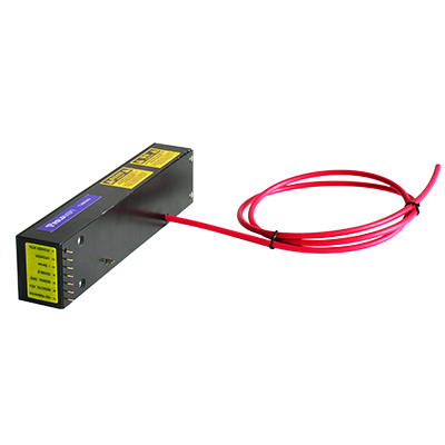
Miniaturization of power supply assemblies has become important as semiconductor equipment designs seek to minimize footprint and reduce gas volume in vacuum process chambers. Compact power supply designs using advanced power electronics topologies and high-density packaging techniques deliver required performance in volumes substantially smaller than traditional designs, supporting integration into process chambers rather than remote mounting in equipment racks. Space savings from compact power supply designs contribute to overall equipment miniaturization trends that reduce facility footprints and construction costs for semiconductor manufacturing facilities.
Electromagnetic interference generated by electrostatic chuck power supplies must be controlled to prevent interference with sensitive process monitoring instruments operating in close proximity. Switching regulator designs inherently generate electromagnetic emissions that require filtering and shielding to meet compatibility requirements. Advanced designs employ spread-spectrum switching techniques and sophisticated filtering to minimize interference signatures while maintaining power supply performance. Electromagnetic compatibility verification ensures that power supply operation does not degrade performance of adjacent measurement systems essential for process control.
Reliability requirements for semiconductor manufacturing equipment demand exceptional lifetime performance from electrostatic chuck power supplies. Production environments operate continuously, with equipment uptime directly impacting manufacturing economics. Power supply designs emphasize robust components, conservative derating, and thorough thermal management to achieve operational lifetimes extending across multiple years of continuous production operation without requiring maintenance intervention. Reliability engineering practices including failure mode analysis and design for manufacturability ensure consistent power supply performance throughout equipment lifetime.
Future process developments will continue to challenge electrostatic chuck power supply capabilities, with trends toward higher operating temperatures, larger wafer diameters, and more complex wafer structures requiring ongoing advancement in power supply technology. Research into chuck materials, electrode configurations, and control algorithms will drive corresponding evolution in power supply designs, ensuring that these essential components continue supporting advancement in semiconductor manufacturing capability.