Application of High-Voltage X-Ray Sources in PCB Inspection
PCB (Printed Circuit Board) is the abbreviation of printed circuit board, which is one of the most important components in electronic products. PCB inspection is an important step in ensuring PCB quality, mainly used to detect PCB defects, such as short circuits, open circuits, and poor soldering.
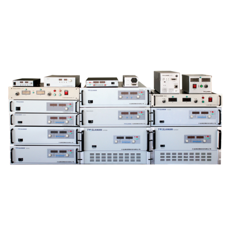
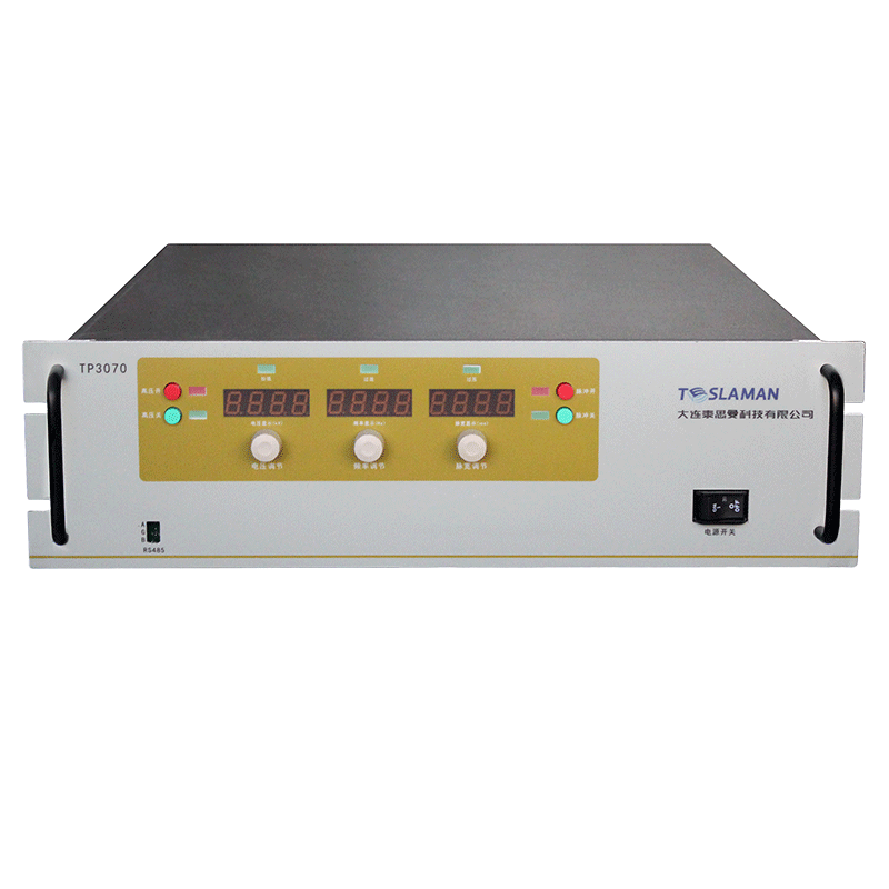
High-voltage X-ray sources are an important part of X-ray generators, which have a wide range of applications in PCB inspection. High-voltage X-ray sources generate X-rays by applying high voltage to an X-ray tube. When X-rays pass through the PCB, they are absorbed or scattered by defects in the PCB, resulting in an image.
The advantages of high-voltage X-ray sources in PCB inspection are mainly reflected in the following aspects:
High sensitivity: High-voltage X-ray sources can detect very small defects in the PCB, such as short circuits and open circuits.
High accuracy: High-voltage X-ray sources can accurately locate defects in the PCB.
Fast speed: High-voltage X-ray sources can quickly inspect PCBs.
The main applications of high-voltage X-ray sources in PCB inspection include:
Defect detection: High-voltage X-ray sources can detect defects in the PCB, such as short circuits, open circuits, and poor soldering. These defects are common in PCBs and have a significant impact on PCB performance and reliability.
Thickness measurement: High-voltage X-ray sources can measure the thickness of PCBs. This application is mainly used in PCB design and manufacturing to ensure that PCB thickness meets design requirements.
Material analysis: High-voltage X-ray sources can analyze the material composition of PCBs. This application is mainly used in PCB research and design to understand the material properties of PCBs.
The application of high-voltage X-ray sources in PCB inspection is becoming increasingly widespread, becoming an important means of PCB inspection. With the continuous development of high-voltage X-ray source technology, the application of high-voltage X-ray sources in PCB inspection will become more in-depth and extensive.
Advantages of high-voltage X-ray sources in PCB inspection
The advantages of high-voltage X-ray sources in PCB inspection are mainly reflected in the following aspects:
High sensitivity: High-voltage X-ray sources can detect very small defects in the PCB, such as short circuits and open circuits. This is mainly because X-rays have strong penetration, which can penetrate the insulation layer and conductor of the PCB, and be absorbed or scattered by defects in the PCB.
High accuracy: High-voltage X-ray sources can accurately locate defects in the PCB. This is because the penetration ability of X-rays is controllable. By adjusting the energy of X-rays, the positioning accuracy of X-rays on PCB defects can be improved.
Fast speed: High-voltage X-ray sources can quickly inspect PCBs. This is because the penetration speed of X-rays is very fast, which can instantly penetrate the PCB and form an image.
Types of applications of high-voltage X-ray sources in PCB inspection
The main applications of high-voltage X-ray sources in PCB inspection include the following types:
Defect detection: High-voltage X-ray sources can detect defects in the PCB, such as short circuits, open circuits, and poor soldering. These defects are common in PCBs and have a significant impact on PCB performance and reliability.
Thickness measurement: High-voltage X-ray sources can measure the thickness of PCBs. This application is mainly used in PCB design and manufacturing to ensure that PCB thickness meets design requirements.
Material analysis: High-voltage X-ray sources can analyze the material composition of PCBs. This application is mainly used in PCB research and design to understand the material properties of PCBs.
Future development trends of high-voltage X-ray sources in PCB inspection
With the continuous development of high-voltage X-ray source technology, the application of high-voltage X-ray sources in PCB inspection will become more in-depth and extensive. In the future, the application of high-voltage X-ray sources in PCB inspection will be developed in the following directions:
Improved sensitivity: The sensitivity of high-voltage X-ray sources will be further improved, enabling the detection of smaller defects in PCBs.
Improved accuracy: The accuracy of high-voltage X-ray sources will be further improved, enabling more accurate localization of defects in PCBs.
Improved speed: The speed of high-voltage X-ray sources will be further improved, enabling faster inspection of PCBs.
Reduced cost: The cost of high-voltage