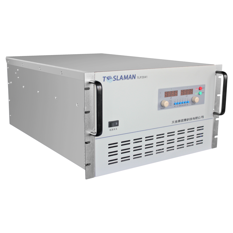
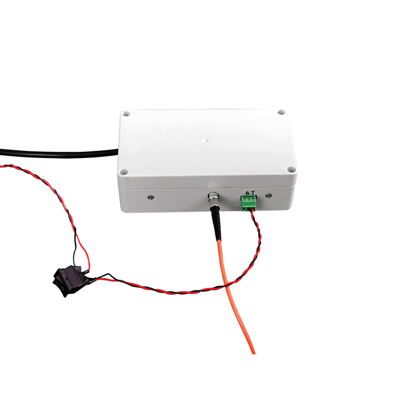
Etching Equipment High Voltage Power Supply Low Power Mode in Atomic Layer Etching
The atomic layer etching process represents the ultimate precision in material removal technology, requiring exceptional control over the etching conditions at the atomic scale. The high voltage power supply in atomic layer etching equipment must operate in a low power mode that delivers precisely controlled energy to the plasma while maintaining the process conditions required for self-limiting etching behavior. Over five decades of experience with high voltage systems in semiconductor processing have demonstrated that the low power mode presents unique design challenges that differ from conventional plasma power supply applications. The power supply must provide stable operation at power levels that are orders of magnitude lower than typical etching processes while maintaining the precision and reliability required for semiconductor manufacturing.
The atomic layer etching process alternates between surface modification steps and removal steps to achieve layer-by-layer material removal. The surface modification step typically uses a reactive gas plasma that is generated by a radio frequency power supply. The removal step uses a low energy ion bombardment that is controlled by a bias voltage applied to the substrate. The high voltage power supply for the bias application must operate at low power levels to prevent damage to the substrate and to maintain the self-limiting nature of the etching process.
The power level requirements for atomic layer etching are typically in the range of tens to hundreds of watts, which is significantly lower than the kilowatt-level power used in conventional plasma etching. The low power operation requires careful design of the power supply output stage to maintain efficiency and stability at reduced power levels. The switching elements must be designed to operate with minimal losses at the reduced current levels. The control loop must be designed to maintain stability at the low power levels where the parasitic elements of the circuit can have a significant effect on the performance.
The voltage control at low power levels requires accurate measurement of the output voltage and current. The measurement sensors must be designed to provide accurate readings at the reduced signal levels. The voltage divider and the current shunt must be designed to minimize the loading effect on the output. The measurement accuracy determines the precision of the power control, which is critical for the repeatability of the atomic layer etching process.
The impedance matching between the power supply and the plasma load is critical for efficient power delivery at low power levels. The plasma impedance varies with the power level, the gas composition, and the pressure. The matching network must be designed to provide the impedance transformation over the range of operating conditions. The matching network components must be rated for the voltage and current levels encountered in the low power operation.
The plasma ignition at low power levels requires special attention because the plasma may not ignite reliably at reduced power. The power supply must provide a higher ignition voltage that is applied momentarily to initiate the plasma, followed by a reduction to the operating power level. The ignition sequence must be controlled precisely to prevent damage to the substrate and to ensure consistent plasma conditions. The ignition voltage must be generated by the power supply without exceeding the voltage rating of the system components.
The pulse mode operation is commonly used in atomic layer etching to control the ion energy and the flux independently. The power supply must provide pulsed output with precise control of the pulse width, the pulse repetition rate, and the pulse amplitude. The pulse parameters determine the ion energy distribution and the etching rate. The power supply must respond to the pulse control signals with minimal delay and with consistent pulse characteristics from pulse to pulse.
The bias voltage control during the removal step determines the ion energy that bombards the substrate surface. The bias voltage must be controlled precisely to achieve the desired ion energy without causing damage to the substrate. The bias voltage is typically in the range of tens to hundreds of volts, which is lower than the voltage used in conventional etching processes. The bias power supply must provide stable voltage output with low ripple and noise to maintain the ion energy uniformity.
The temperature control of the substrate during atomic layer etching is critical for the process uniformity and the self-limiting behavior. The substrate temperature must be maintained within a narrow range to achieve the consistent etching rate. The high voltage power supply generates heat that must be dissipated without affecting the substrate temperature. The power supply cooling system must be designed to prevent heat transfer to the substrate and to maintain the temperature stability of the process chamber.
The gas delivery system for atomic layer etching must provide precise control of the gas flow rates and the gas composition. The gas flow is controlled by mass flow controllers that are regulated by the process control system. The gas pressure in the process chamber affects the plasma characteristics and the etching rate. The high voltage power supply must be interlocked with the gas delivery system to prevent operation without the proper gas flow and pressure.
The end-point detection for atomic layer etching requires sensitive measurement techniques that can detect the removal of a single atomic layer. The detection system may use optical emission spectroscopy, mass spectrometry, or ellipsometry to monitor the etching process. The high voltage power supply must provide stable conditions for the end-point detection system to operate reliably. The power supply noise must be minimized to prevent interference with the sensitive detection measurements.
The process control system for atomic layer etching must integrate the information from multiple sensors to maintain the process parameters within the specified range. The control system must coordinate the gas delivery, the plasma generation, the bias voltage, and the substrate temperature to achieve the desired etching results. The control algorithm must be designed to maintain the self-limiting behavior of the etching process while responding to the disturbances that occur during the process.
The low power mode of the high voltage power supply in atomic layer etching equipment requires specialized design approaches that address the unique requirements of the process. The power supply must provide stable operation at reduced power levels while maintaining the precision and reliability required for semiconductor manufacturing. The experience gained from decades of high voltage power supply development for plasma processing provides the foundation for the continued advancement of atomic layer etching technology. The integration of the power supply with the overall process control system enables the precise control of the etching conditions that is required for atomic-level material removal.