Microchannel Plate Detector High Voltage Power Supply Temperature Compensation Circuit Design
Microchannel plate detectors are essential components in a wide range of scientific instruments, including mass spectrometers, electron microscopes, astronomical telescopes, and time-of-flight analyzers. These detectors amplify weak signals of charged particles or photons through a cascade of secondary electron emissions within microscopic channels, achieving gain factors of 10 million or more. The high voltage power supply that biases the microchannel plate is critical for maintaining a stable gain across the detector surface and over time. Temperature variations can cause significant changes in the microchannel plate resistance and the secondary electron emission coefficient, leading to gain drift and measurement errors. The design of temperature compensation circuits for the high voltage power supply is essential for achieving the stability and accuracy required by modern analytical instruments.
The microchannel plate consists of an array of millions of microscopic glass channels, each with a diameter of 10 to 25 micrometers and a length-to-diameter ratio of 40 to 100. The channel walls are treated to have a semiconductor coating that provides the electrical conductivity required for the charge replenishment. The resistance of the microchannel plate, typically in the range of 100 megohms to 1000 megohms, exhibits a strong negative temperature coefficient, decreasing by approximately 1 percent per degree Celsius as the temperature increases. This temperature dependence of the plate resistance causes the bias voltage across the plate to change with temperature when the power supply operates in a constant voltage mode, leading to variations in the detector gain.
The temperature compensation circuit for the microchannel plate high voltage power supply must account for the temperature dependence of both the plate resistance and the secondary electron emission coefficient. The gain of the microchannel plate is approximately proportional to the bias voltage raised to the power of 8 to 10, meaning that a small change in the bias voltage causes a large change in the gain. For a typical microchannel plate with a gain of 10 million at 1000 V, a 1 percent change in the bias voltage can cause a 10 percent change in the gain. The temperature compensation circuit must maintain the gain within 1 percent over the operating temperature range to ensure the accuracy of the measurements.
The primary approach to temperature compensation involves sensing the temperature of the microchannel plate and adjusting the bias voltage to compensate for the temperature-dependent gain variations. The temperature sensor, typically a thermistor or a platinum resistance temperature detector, is mounted in thermal contact with the microchannel plate or the detector housing. The sensor output is processed by the compensation circuit, which generates a correction signal that adjusts the high voltage power supply output. The compensation circuit must be designed with the appropriate transfer function to match the temperature dependence of the microchannel plate gain.
The transfer function of the temperature compensation circuit is determined by the characteristics of the specific microchannel plate and the operating conditions. The compensation circuit typically implements a polynomial or piecewise linear function that relates the temperature to the required bias voltage correction. The coefficients of the compensation function are determined through calibration measurements that characterize the gain of the microchannel plate as a function of temperature and bias voltage. The calibration is performed by measuring the detector response at several temperatures and bias voltages, and fitting the data to the compensation model.
The analog implementation of the temperature compensation circuit uses operational amplifiers and precision resistors to generate the correction signal. The temperature sensor is connected in a bridge circuit that produces a voltage proportional to the temperature deviation from a reference temperature. The bridge output is amplified and processed through a shaping circuit that implements the compensation transfer function. The correction signal is then summed with the bias voltage setpoint to produce the compensated output voltage. The analog circuit must be designed with low drift and low noise to avoid introducing errors into the bias voltage.
The digital implementation of the temperature compensation circuit offers greater flexibility and precision compared to the analog approach. The temperature sensor output is digitized by an analog-to-digital converter, and the compensation algorithm is implemented in a microcontroller or a digital signal processor. The compensation function can be stored in a lookup table or calculated using polynomial equations, allowing the compensation to be tailored to the specific microchannel plate installed in the detector. The digital implementation also allows the compensation parameters to be updated through a communication interface, simplifying the calibration procedure and enabling adaptive compensation that adjusts to the aging of the microchannel plate.
The thermal design of the detector housing and the power supply must minimize the temperature gradients that can cause non-uniform gain across the microchannel plate surface. The temperature sensor must be located at a position that is representative of the average temperature of the microchannel plate, and the thermal coupling between the sensor and the plate must be sufficient to ensure accurate temperature measurement. The detector housing should be designed with uniform thermal mass and good thermal conductivity to minimize temperature gradients. The power supply components that generate heat should be located away from the detector to avoid creating local temperature hot spots.
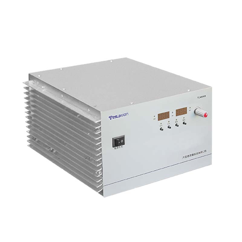
The high voltage power supply for the microchannel plate must provide a stable output voltage that can be adjusted by the temperature compensation circuit. The power supply output voltage range must be sufficient to accommodate the required bias voltage and the compensation range, typically 500 V to 2000 V for a single microchannel plate or up to 4000 V for a stack of two or three plates. The power supply must have a resolution of better than 1 V to allow fine adjustment of the bias voltage for gain compensation. The output voltage ripple must be less than 10 mV peak-to-peak to avoid introducing noise into the detector signal.
The response time of the temperature compensation circuit must be matched to the thermal time constant of the microchannel plate. The thermal time constant of a typical microchannel plate is on the order of several minutes, depending on the plate size and the mounting configuration. The compensation circuit must respond to temperature changes on a time scale that is faster than the thermal time constant to prevent gain drift, but not so fast that it responds to short-term temperature fluctuations that are not representative of the plate temperature. The compensation circuit bandwidth is typically set to 0.1 Hz to 1 Hz to provide effective compensation without introducing noise.
The stability of the temperature compensation circuit over time is essential for maintaining the calibration of the detector. The components of the compensation circuit, including the temperature sensor, the reference voltage, and the amplification circuits, must have low drift over time and temperature. The temperature sensor must be aged and stabilized before use to minimize drift. The reference voltage source must have a temperature coefficient of less than 1 part per million per degree Celsius to ensure that the compensation accuracy is not degraded by the reference drift. The compensation circuit should be periodically recalibrated to correct for any long-term drift in the component characteristics.
The temperature compensation circuit must be designed to operate reliably in the vacuum environment of the detector. The components must be selected for low outgassing and compatibility with the vacuum environment. The circuit must be designed to dissipate minimal heat to avoid affecting the detector temperature. The high voltage connections between the power supply and the microchannel plate must be designed to minimize leakage currents and corona discharge in the vacuum environment. The insulating materials used in the high voltage feedthroughs and cables must be compatible with the vacuum and must not degrade under the influence of the electric field and the radiation from the detector.
The integration of the temperature compensation circuit with the overall detector control system enables sophisticated monitoring and diagnostic capabilities. The compensation circuit can provide real-time information about the detector temperature, the bias voltage, and the compensation correction, allowing the control system to monitor the detector status and to detect potential problems. The compensation parameters can be stored in the detector memory and automatically loaded when the detector is powered on, ensuring consistent operation across different operating sessions. The temperature compensation data can be logged for quality assurance and for troubleshooting purposes.