Electron Beam System High Voltage Power Supply in MEMS Processing
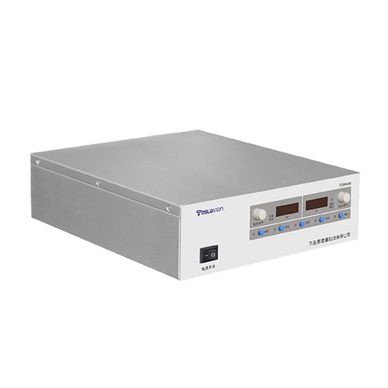
Micro-electro-mechanical systems processing encompasses a suite of fabrication techniques that produce miniature mechanical and electrical structures on silicon and other substrates. Among these techniques, electron beam processing stands out for its ability to pattern, deposit, and modify materials with sub-micrometer precision. The high voltage power supply forms the foundation of electron beam systems for MEMS processing, providing the accelerating potential that determines the energy and resolution of the electron beam. The power supply must deliver stable, precisely controlled voltage across a wide range of operating conditions to support the diverse requirements of MEMS fabrication processes, including electron beam lithography, electron beam induced deposition, and electron beam etching.
The accelerating voltage requirements for MEMS electron beam processing typically range from 1 kilovolt to 100 kilovolts, depending on the specific application. For lithography applications, lower voltages in the 1 to 10 kilovolt range are used to minimize electron scattering in the resist layer, achieving higher resolution patterning. For deposition and etching applications, higher voltages in the 30 to 100 kilovolt range provide the energy needed to drive physical and chemical interactions at the substrate surface. The power supply must cover this wide voltage range with high regulation accuracy, typically better than 0.01 percent, to ensure consistent beam properties across all operating modes. The voltage programming capability allows the beam energy to be adjusted dynamically during processing, which is essential for multi-step fabrication sequences that require different beam energies at each step. Advanced systems also support continuous voltage ramping during processing, enabling graded energy deposition for applications such as three-dimensional microstructure fabrication.
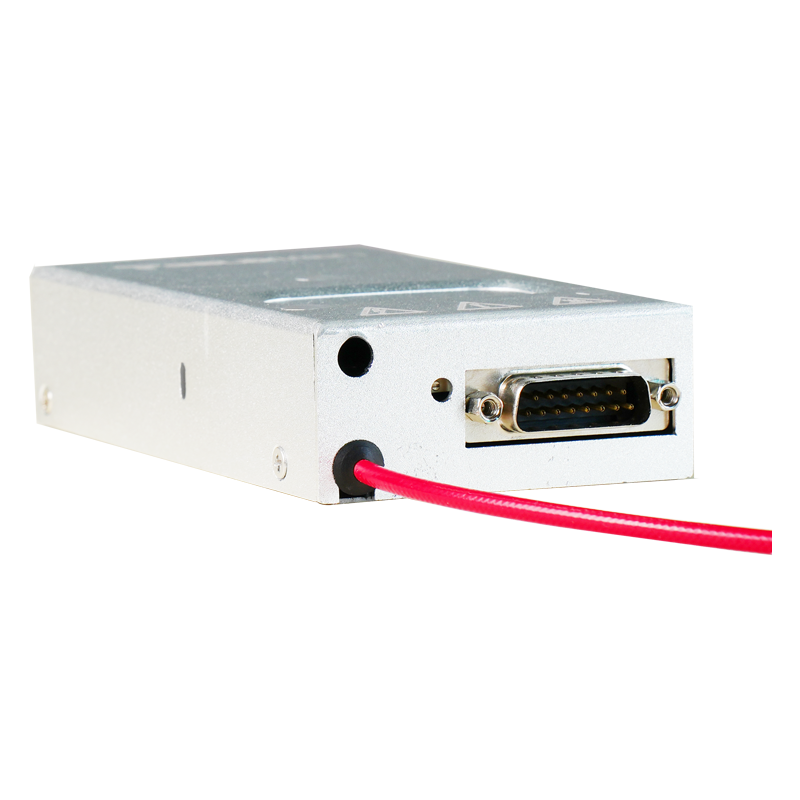
The architecture of electron beam power supplies for MEMS processing incorporates several key design elements. A high frequency inverter converts the mains supply to a high frequency alternating current, typically operating between 20 and 50 kilohertz. This high frequency drives a step-up transformer that provides the initial voltage boost. A multi-stage voltage multiplier then increases the voltage to the final operating level. The output stage includes high voltage filtering capacitors that reduce ripple to levels below 0.01 percent, ensuring the electron beam has minimal energy spread. The entire high voltage section is enclosed in a grounded metal cage to prevent electrical arcing and provide electromagnetic shielding. The transformer design uses a toroidal core with optimized winding geometry to minimize leakage inductance and maximize coupling efficiency, contributing to the overall energy efficiency of the power supply.
Beam current control represents another critical function of the power supply in MEMS processing. The beam current, which can range from picoamps for lithography to microamps for deposition, must be precisely regulated to control the dose delivered to the substrate. The power supply incorporates a separate current regulation loop that adjusts the filament current and grid voltage of the electron gun to maintain the target beam current. Current regulation accuracy better than 0.1 percent is required, particularly for lithography applications where dose uniformity directly impacts pattern fidelity. The power supply also provides beam blanking capability through a high voltage switching circuit that can deflect the beam away from the substrate at specific points during processing, allowing precise patterning of complex structures. The blanking circuit operates at speeds up to several megahertz, enabling accurate patterning with feature sizes approaching the resolution limit of the electron beam system.
Integration with the MEMS processing control system is achieved through high-speed digital communication interfaces. The power supply receives voltage and current commands from the process controller and provides real-time feedback on output parameters. This enables synchronized operation between the electron beam and other process components such as the substrate stage positioning system and the gas delivery system for deposition or etching. The control system can also monitor the power supply status for early detection of potential issues, such as transformer temperature or capacitor leakage, allowing proactive maintenance to prevent unplanned downtime. The combination of precise voltage regulation, flexible current control, and seamless system integration makes modern electron beam power supplies indispensable tools for advanced MEMS fabrication. The integration also extends to the design of proximity effect correction algorithms, where the power supply voltage can be modulated during exposure to compensate for electron scattering effects, improving the fidelity of nanoscale patterns.
The electron beam power supply must also handle the demanding requirements of production MEMS facilities where throughput and uptime are critical. The power supply design incorporates modular components that can be replaced quickly during scheduled maintenance, minimizing equipment downtime. Advanced diagnostic systems monitor the health of critical components including transformer windings, high voltage capacitors, and semiconductor switches, providing early warning of potential failures. Mean time between failure values exceeding 50,000 hours are required for production environments, supported by comprehensive thermal management and component derating. The power supply also includes built-in calibration routines that verify output accuracy against internal reference standards, with automatic compensation for component drift over time. These features ensure that the electron beam power supply maintains its performance specifications throughout its operational life, supporting the high productivity requirements of MEMS manufacturing.
The evolution of electron beam power supply technology continues to address the demands of next-generation MEMS fabrication. Newer designs incorporate digital signal processing for more precise voltage and current control, with faster response times for beam switching and blanking. Multi-channel power supply architectures support multi-column electron beam systems that can process multiple substrates simultaneously, significantly increasing throughput for high-volume manufacturing. Integration with artificial intelligence systems enables adaptive voltage control that optimizes beam parameters based on real-time feedback from the process monitoring system, further improving pattern fidelity and process efficiency. These technological advances position the electron beam power supply as a critical enabling component for the continued scaling of MEMS device complexity and performance.
The safety design of electron beam power supplies addresses the hazards of high voltage operation and electron beam generation. The power supply chassis incorporates multiple independent insulation layers and controlled discharge paths to prevent accidental exposure. The electron gun assembly includes interlock systems that disable the high voltage when the vacuum level drops below a safe threshold or when any service access panel is opened. X-ray shielding around the electron beam path attenuates bremsstrahlung radiation to levels well below occupational exposure limits. The power supply also monitors internal gas pressure and temperature, initiating controlled shutdown sequences if any unsafe condition is detected. These comprehensive safety features ensure that the electron beam MEMS processing system meets all regulatory requirements for safe operation in research and production environments.