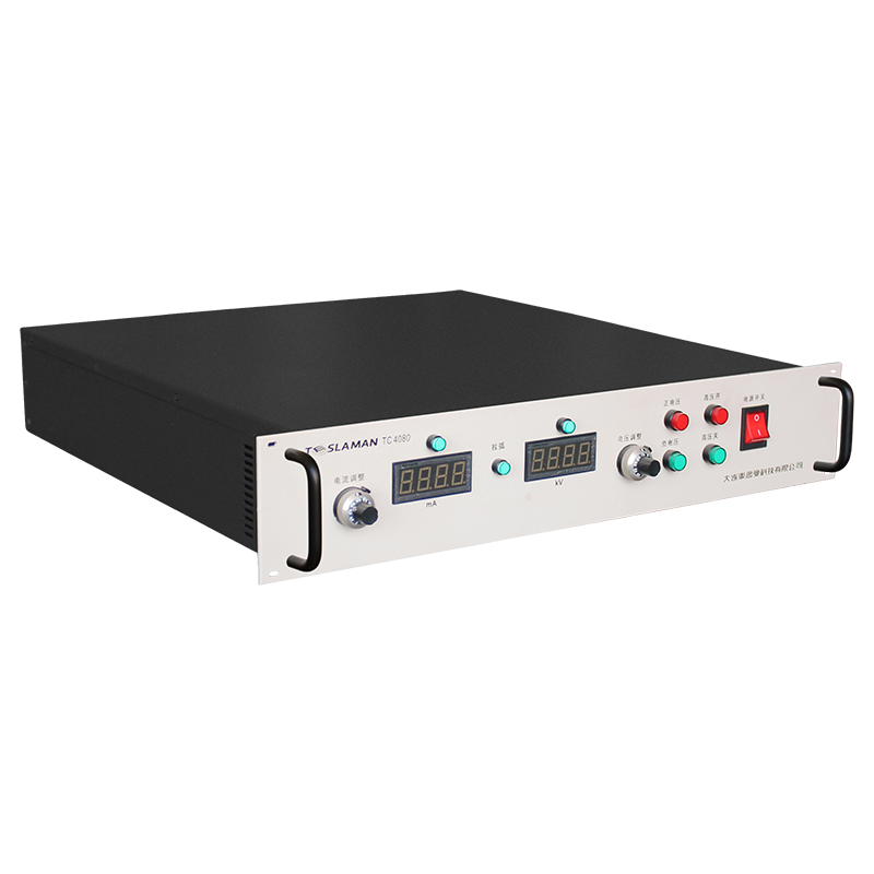
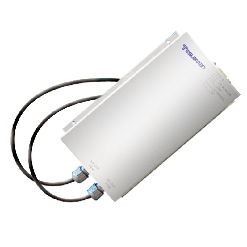
Lithography High Voltage Power Supply in Multi-Patterning Process Synchronous Control
Multi-patterning lithography represents a cornerstone technology in advanced semiconductor manufacturing, enabling the creation of sub-10nm feature sizes through successive exposure and etch cycles. At the heart of this intricate process lies the high voltage power supply, which governs the operation of critical subsystems including the electron beam column, the wafer chuck electrostatic clamping mechanism, and the detector assembly for alignment and focus measurements. The synchronization of these subsystems demands exceptional power supply performance, characterized by ultra-low ripple, rapid transient response, and precise voltage regulation across a wide range of operating conditions.
The multi-patterning workflow typically involves double or quadruple patterning schemes, where each lithography step requires independent high voltage operation for pattern transfer. The first patterning cycle establishes the initial layer of features on the wafer surface, while subsequent cycles refine and augment these features to achieve the desired density and resolution. Each cycle demands that the high voltage power supply maintain stable output during wafer positioning, exposure, and alignment verification phases. Even minor voltage fluctuations during exposure can lead to critical dimension variations that propagate through the entire manufacturing chain, ultimately affecting device performance and yield.
Synchronous control represents the most challenging aspect of high voltage operation in multi-patterning lithography. The power supply must coordinate voltage transitions with the wafer stage positioning system, the optical alignment sensors, and the exposure source modulation. When a wafer moves from one exposure field to the next, the high voltage supply must adjust its output to meet the power requirements of the new field location, accounting for variations in chuck capacitance, temperature coefficients, and electrical loading. This adjustment must occur within microsecond timescales to avoid introducing alignment errors or focus offsets that would compromise pattern fidelity.
The electron beam column in e-beam lithography requires multiple high voltage rails operating at different potential levels. The cathode typically operates at negative potentials ranging from -5kV to -100kV, while the extractor and focusing elements operate at intermediate voltages. Each rail must be independently regulated with stability better than 0.001 percent over extended periods, and the voltage tracking between rails must be maintained to ensure proper beam focusing and deflection. During multi-patterning, the electron beam may need to switch between different acceleration voltages for each patterning layer, requiring the power supply to transition between operating points without significant overshoot or ringing.
The wafer chuck electrostatic clamping system represents another critical high voltage application in lithography. Advanced chucks use dual-polarity electrostatic clamping, where positive and negative voltage electrodes create an electrostatic field that holds the wafer in place during exposure. The clamping force is directly proportional to the square of the applied voltage, making voltage regulation paramount for maintaining uniform clamping across the wafer surface. During multi-patterning, the chuck must maintain consistent clamping force as the wafer undergoes multiple thermal cycles and mechanical handling steps, requiring the high voltage supply to compensate for changes in chuck capacitance and leakage current.
Detector systems used for alignment and focus measurements also rely on high voltage power supplies. Secondary electron detectors, backscattered electron detectors, and optical sensors all require bias voltages and acceleration potentials that must remain stable throughout the measurement sequence. In multi-patterning, alignment marks from previous layers must be detected with sub-nanometer precision, which demands that the detector high voltage supplies exhibit exceptionally low noise floors and minimal drift over time. The synchronization between detector voltage adjustment and alignment signal acquisition must be carefully engineered to avoid introducing phase shifts or timing errors.
The control architecture for multi-patterning high voltage systems typically employs a distributed control scheme with local regulation loops and a central synchronization controller. Each high voltage rail features its own voltage feedback loop with high-precision analog-to-digital conversion, while the central controller coordinates the operation of all rails based on process timing signals derived from the lithography tool's main controller. This architecture enables independent regulation of each voltage rail while ensuring coordinated transitions during critical process steps. The synchronization controller receives trigger signals from the wafer stage encoder, the exposure source modulator, and the alignment sensor, and generates voltage transition commands that account for the specific requirements of each patterning cycle.
Thermal management constitutes a significant challenge for high voltage power supplies in multi-patterning lithography. The power dissipation in high voltage regulators, even at low load currents, can lead to temperature rises that affect component characteristics and voltage stability. Advanced thermal design employs liquid cooling with precise temperature control, heat exchangers with high thermal conductivity materials, and thermal modeling to predict temperature distributions across the power supply module. The thermal control system must maintain the power supply within a narrow temperature range throughout the multi-patterning sequence, as temperature-induced voltage offsets would accumulate across successive patterning cycles and compromise overlay accuracy.
In summary, the high voltage power supply in multi-patterning lithography embodies the pinnacle of power supply engineering, combining ultra-high precision, rapid dynamic response, and exceptional long-term stability. Its role in synchronous control across multiple subsystems makes it indispensable for achieving the stringent requirements of advanced semiconductor manufacturing. The continuous development of multi-patterning techniques drives the evolution of high voltage power supply technology, pushing the boundaries of what is achievable in terms of voltage regulation, transient performance, and system integration.