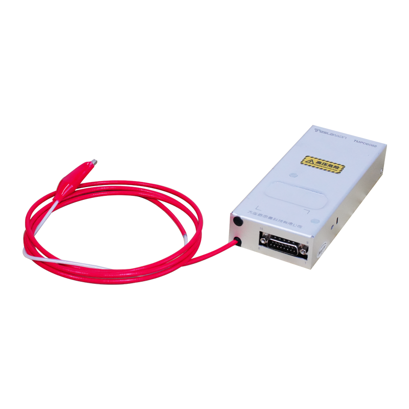
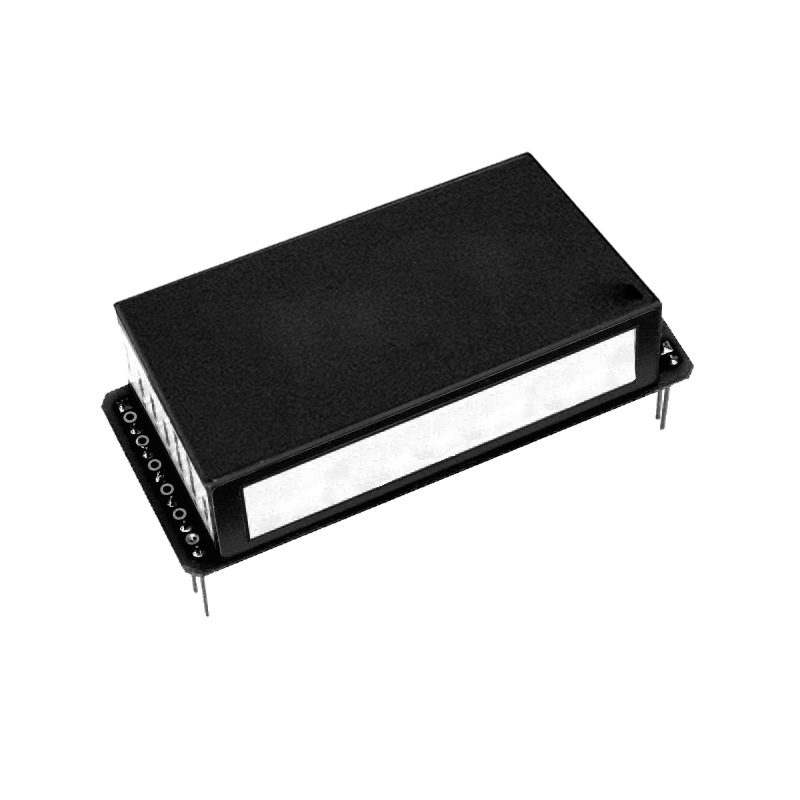
E-CHUCK High Voltage Power Supply Adsorption Precision in Advanced Packaging Technology
Electrostatic chucks have become indispensable in advanced semiconductor packaging, providing precise and reliable wafer holding during critical manufacturing operations. The E-CHUCK uses electrostatic attraction generated by a high voltage electric field to secure wafers in place, offering significant advantages over conventional mechanical clamping methods. The high voltage power supply serves as the core component that generates and regulates the electrostatic field, and its adsorption precision directly influences the quality and yield of advanced packaging processes.
Advanced packaging technologies such as flip chip bonding, wafer-level packaging, and 3D stacking require extremely precise wafer positioning and retention during processing. The E-CHUCK addresses these requirements by providing uniform, controllable electrostatic clamping that eliminates mechanical stress and contamination risks associated with traditional clamping methods. The high voltage power supply generates the electric field that creates the electrostatic attraction between the chuck and the wafer, with the clamping force directly proportional to the square of the applied voltage.
The E-CHUCK high voltage power supply typically operates at voltages ranging from 500V to 5kV, with the specific voltage determined by the chuck design, wafer type, and process requirements. The power supply must deliver this voltage with exceptional stability, as voltage fluctuations directly affect the clamping force uniformity across the wafer surface. Voltage stability better than 0.01 percent is required to ensure uniform adsorption across the entire wafer, preventing localized stress or wafer movement during processing.
Dual-polarity E-CHUCK designs, which use both positive and negative electrodes, offer more precise control of the electrostatic field distribution. The high voltage power supply for dual-polarity chucks must provide independent regulation of positive and negative voltage rails, enabling the creation of complex field patterns that can compensate for wafer topography variations and achieve more uniform clamping. The ability to adjust the voltage on individual electrode segments further enhances the precision of the adsorption force distribution, which is particularly important for large-diameter wafers where edge effects become significant.
The adsorption precision of the E-CHUCK is determined by several factors related to the high voltage power supply performance. Voltage regulation accuracy ensures that the target voltage is maintained consistently, while ripple and noise levels determine the smoothness of the electrostatic field. The transient response capability of the power supply allows rapid adjustment of the clamping force in response to changing process conditions, such as temperature variations or wafer surface property changes. All these factors must be optimized to achieve the sub-micron positioning stability required for advanced packaging operations.
Temperature control is closely linked to E-CHUCK performance, as the electrostatic clamping force varies with temperature due to changes in wafer resistivity and chuck material properties. The high voltage power supply must incorporate temperature compensation circuits that adjust the output voltage based on the measured chuck and wafer temperatures, maintaining a constant clamping force throughout the thermal processing cycle. This temperature compensation is particularly critical during operations such as bonding and curing, where wafer temperatures can vary significantly.
The E-CHUCK power supply must also account for the dielectric properties of the wafer and any intermediate layers. Different wafer materials, including silicon, germanium, and compound semiconductors, exhibit different dielectric constants and resistivity values, which affect the electrostatic field distribution and clamping force. The power supply's control system can store material-specific parameters and adjust the voltage accordingly when switching between wafer types, ensuring consistent adsorption performance across different product lines.
Advanced packaging processes often involve multiple thermal and mechanical cycles, during which the wafer must remain securely clamped. The high voltage power supply must maintain stable output throughout these cycles, compensating for changes in chuck capacitance, wafer charge accumulation, and leakage current. The power supply's monitoring system continuously measures the clamping current and voltage, detecting any anomalies that may indicate wafer de-chucking or loss of adsorption force. When anomalies are detected, the system can automatically adjust the voltage or generate alarms to alert operators.
Safety considerations are paramount in E-CHUCK high voltage power supply design. The chuck operates at elevated voltages in close proximity to sensitive semiconductor devices, requiring comprehensive electrical safety features. The power supply must incorporate leakage current detection, ground fault protection, and emergency discharge circuitry to prevent damage to wafers or equipment in the event of electrical faults. Additionally, the E-CHUCK design must include charge removal circuits that safely dissipate the electrostatic charge after processing, preventing electrical discharge damage to the wafer during unloading.
Integration with the packaging tool's control system enables closed-loop optimization of E-CHUCK performance. The control system receives real-time data from the high voltage power supply, including voltage, current, temperature, and clamping force measurements, and uses this information to adjust process parameters. Machine learning algorithms can be employed to identify optimal voltage settings for different wafer types and process conditions, further enhancing the adsorption precision and reliability of the E-CHUCK system.
The latest generation of E-CHUCK power supplies incorporates digital control technology with advanced signal processing capabilities. Digital signal processors enable precise voltage regulation with minimal overshoot and ringing, while high-resolution analog-to-digital converters provide accurate feedback of the output voltage and current. These digital control systems also support remote monitoring and diagnostics, enabling predictive maintenance and reducing equipment downtime in advanced packaging facilities.
In conclusion, the E-CHUCK high voltage power supply represents a critical enabling technology for advanced semiconductor packaging. Its ability to deliver precise, stable electrostatic clamping force with sub-micron positioning accuracy is essential for achieving the high yield and quality requirements of modern packaging processes. As advanced packaging technology continues to evolve toward higher levels of integration and performance, the E-CHUCK power supply will remain at the forefront of innovation, supporting the development of increasingly sophisticated semiconductor devices for diverse applications.