High-Voltage Stability of Light Source Power Supplies in Extreme Ultraviolet Lithography
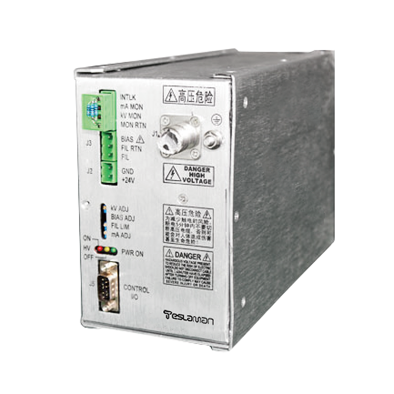
Extreme ultraviolet lithography relies on a light source that produces radiation at a wavelength of 13.5 nanometers, and the generation of this radiation places extraordinary demands on the high-voltage systems that feed the source. In laser-produced plasma sources, a high-energy carbon dioxide laser pulse is focused onto a tin droplet, and the resulting plasma radiates in the EUV band; in discharge-produced plasma sources, a high-current discharge through tin vapor creates the plasma. In both configurations the energy delivered into the plasma must be controlled within tight limits, because the dose uniformity across the wafer directly depends on the pulse-to-pulse energy stability of the source. The high-voltage supply that charges the pulse-forming network is therefore a critical element of the lithography tool, and the stability of this supply determines, to a large extent, the stability of the emitted light.
The pulse energy of the source is set by the electrical energy stored in the pulse capacitor bank. The stored energy scales with the square of the charging voltage, so a small deviation in the charging voltage produces a proportionally larger deviation in the pulse energy. A one percent charging voltage error translates into approximately two percent energy error, which is far beyond the tolerance that a modern scanner can accept. The charging supply must therefore regulate the capacitor voltage with a precision that keeps the energy error within the dose budget of the process, and the regulation must hold across the entire repetition rate range of the source, from low-speed servicing modes to the full production burst rate.
The architecture of the charging supply follows from the pulse characteristics. A resonant charging topology is commonly employed, in which the energy transfer from the input converter to the capacitor bank is governed by a resonant circuit that provides inherent current limiting and high charging efficiency. The charging voltage is sampled through a precision divider, and the control loop terminates the charging at the precise moment the target voltage is reached. Because the capacitor voltage continues to settle after the charging terminates, the termination logic must account for the droop and the overshoot of the final value, and the compensation parameters are calibrated for each capacitor bank configuration.
Voltage ripple and noise on the charged capacitor directly enter the pulse waveform. The ripple components originate from the switching activity of the input converter and from the interactions between the charging circuit and the load network. The filtering of the charging path must be designed with the pulse repetition frequency in mind, because the ripple at the repetition frequency or at harmonics of that frequency will appear as correlated noise in the EUV dose measurements. Shielded layouts, low-inductance capacitor interconnections and careful grounding of the charging stage reduce the noise floor to the level required by the dose control loop.
The timing relationship between the charging phase and the pulse firing is another dimension of stability. The firing command must be delivered at a defined point in the charging cycle, and the jitter of this timing converts into pulse energy variation because the capacitor voltage is still settling when the discharge begins. The trigger circuit that fires the discharge switch must have low jitter and must be immune to the electromagnetic disturbance generated by the discharge itself. Optical triggering is frequently used to decouple the trigger path from the high-voltage noise environment, and the optical link preserves the timing accuracy across the potential barrier.
The power semiconductors in the charging and switching stages operate under severe electrical stress. The charging switch must block the full charging voltage and conduct the charging current, while the discharge switch must close into a near-short circuit and carry the pulse current. Silicon carbide devices are increasingly used for both functions because of the fast switching capability and the high-temperature operation margin. The gate drive circuits must be designed for the high dv/dt and di/dt environment, and the drive timing must be verified under the worst-case load conditions rather than under nominal conditions.
Thermal management of the source power supply is coupled to the thermal environment of the source module. The source area is densely packed with optical elements, vacuum hardware and electronics, and the heat rejected by the power stages must be removed without disturbing the thermal stability of the optics. Liquid cooling is typically required at the power levels involved, and the cooling loops of the power electronics and the optics are kept separate to prevent thermal coupling. The temperature of the charging capacitors influences the capacitance and hence the stored energy, so the capacitor bank is often temperature-controlled to maintain the energy repeatability across environmental variations.
Electromagnetic compatibility inside a lithography scanner is governed by the extreme sensitivity of the metrology systems. The scanner contains interferometers, encoders and image sensors that operate at the nanometer scale, and any electromagnetic disturbance coupled into these systems degrades the overlay and the focus performance. The power supplies of the light source must therefore meet stringent emission limits, and the shielding and filtering measures are verified in the assembled tool rather than on the bench. The grounding architecture of the scanner provides a single reference plane, and the source supplies are connected to this plane with low-impedance straps to prevent potential differences between modules.
Diagnostics and monitoring convert the stability requirement into an operational reality. The charging voltage of every pulse is measured and recorded, and the statistical distribution of the pulse energies is compared with the specification in real time. Drift of the mean energy is compensated by adjusting the charging target, while an increase in the energy variance triggers an investigation of the charging supply and the capacitor bank. The diagnostic data support preventive maintenance, because the degradation of the capacitors and the switches produces characteristic signatures in the energy statistics before the performance falls out of specification.
The long-term stability of the light source supply depends on the aging behavior of the components. The capacitors undergo millions of charge-discharge cycles, and the dielectric losses and the capacitance drift accumulate with the cycle count. The discharge switches experience erosion and contact degradation, and the trigger circuits must be checked periodically. Life-monitoring counters track the number of pulses delivered, and the maintenance schedule is aligned with the component lifetimes derived from accelerated testing. The data from the monitoring systems also feed back into the design of the next-generation source supplies, closing the loop between field experience and product improvement.
The stability of the light source high-voltage supply is thus a multi-layered discipline. The regulation accuracy of the charging loop sets the baseline, the noise and timing performance define the pulse-to-pulse quality, and the thermal and aging control preserve the performance over the service life. Each layer must be engineered with the same precision as the optical system of the scanner, because the dose uniformity that determines the lithographic yield begins with the energy stability of the electrical pulse.