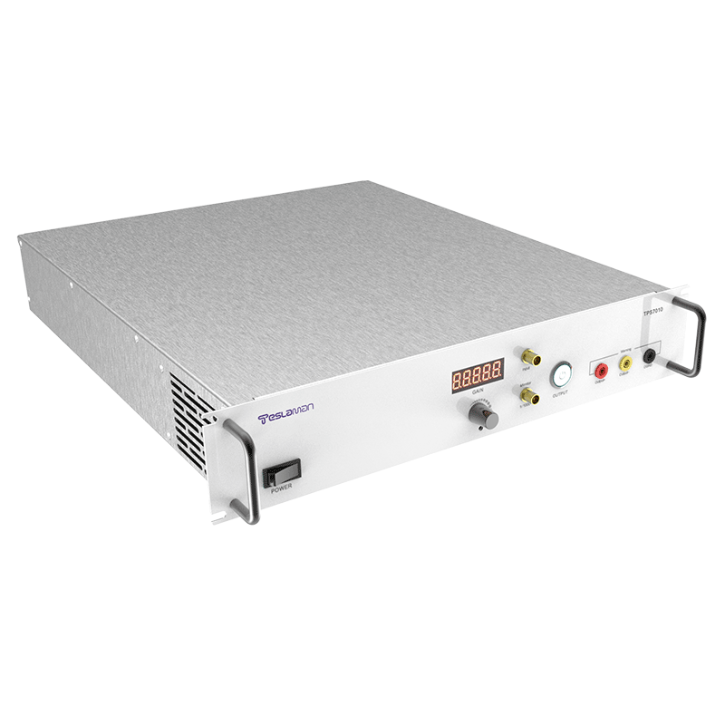
Analysis of High Voltage Power Supply Ionization Efficiency and Optimization Strategies
1. Core Factors Affecting Ionization Efficiency
The ionization efficiency (η) of high-voltage power supplies is defined as the ratio of effective ion kinetic energy to input electrical energy, expressed as:
\[ η = \frac{n_e e E λ}{P_{in}} \times 100\% \]
where \(n_e\) is electron density, \(E\) is electric field strength, and \(λ\) is mean free path. Empirical data show η typically ranges between 15-38% in industrial systems. Key influencing factors include:
1. Field Uniformity: A >20% field deviation in multi-needle-plate electrodes reduces η by 8-12%. Optimizing electrode curvature (0.5-1.2mm radius) expands ionization zones by 40%.
2. Gas Parameter Control: Argon exhibits 17% higher η than nitrogen at 10⁻²Pa vacuum, but η decreases ~5% per order of magnitude increase in gas density.
3. Ripple Characteristics: Output ripple >0.5% causes 3-5% η loss. LCLC filter networks suppress ripple to <0.1%.
2. Efficiency Enhancement Technologies
1. Pulse-Modulated Ionization
High-frequency pulses (1-10MHz) with steep edges (<50ns) exceed Townsend discharge thresholds. 100kV pulses achieve η=42%, while 10μs pulses at 20% duty cycle boost deposition rates by 28%.
Bipolar pulses reduce space charge accumulation by 60%, extending continuous operation cycles 3x.
2. Magnetron Sputtering Synergy
Transverse magnetic fields (0.1-0.3T) spiralize electron paths, raising collision probability by 50%. Multistage structures achieve 85% ionization rates—40% higher than DC sputtering.
RF coupling (13.56MHz) in dielectric barrier discharges achieves 8eV electron temperature and 10¹⁶/m³ ion density for large-area processing.
3. Adaptive Impedance Matching
Dynamic Smith chart algorithms limit reflected power to <0.3% across 10-100kHz. Applied to ion implanters, this improves beam stability to 99.7%.
3. Efficiency Comparison in Applications
| Application | Voltage Range | Operation Mode | η Range | Optimization Methods |
|--------------------|---------------|---------------------|-----------|--------------------------------|
| Mass Spectrometry | 3-8kV | DC Glow Discharge | 18-22% | Pulsed Field Emission |
| Waste Gas Treatment| 20-50kV | Dielectric Barrier | 25-32% | Graded Gap Electrodes |
| Semiconductor Doping| 80-150kV | RF Sputtering | 35-40% | Magnetic Filter Ducts |
| Medical Sterilization| 5-15kV | Corona Discharge | 12-15% | Nanostructured Electrodes |
4. Future Technological Trends
1. Ultrafast Pulses: Sub-nanosecond pulses (<1ns) overcome space charge limitations, with simulations predicting η >50% at 200ps pulse widths.
2. AI Optimization: Deep learning-based discharge pattern recognition systems maintain η fluctuations within ±0.5%.
3. Low-Temperature Plasma Coupling: Microwave excitation (2.45GHz) combined with DC bias elevates electron density by 100x while keeping gas temperatures below 40℃.