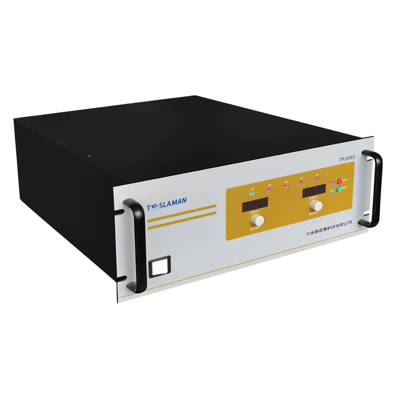
Mechanism and Technological Development of Microscopic Morphology Shaping by Etching High-Voltage Power Supplies
In the precision manufacturing of semiconductor devices, the accurate control of microscopic morphology is a core determinant of device performance. As the energy supply unit in etching processes, high-voltage power supplies directly act on the atomic-level material removal through electric field modulation and plasma generation mechanisms, enabling directional shaping of nanostructures.
1. Electric Field Regulation and Surface Reaction Dynamics
In wet electrochemical etching, high-voltage power supplies adjust the potential difference between anode and cathode to control ion migration rates and redox reaction kinetics in electrolyte solutions. When the voltage gradient reaches a critical threshold, the chemical bond-breaking efficiency on specific crystal planes of the semiconductor surface significantly increases, resulting in anisotropic etching. For instance, pulsed high-voltage output can achieve periodic reaction-passivation cycles, suppressing lateral etching diffusion to form high-aspect-ratio trench structures. During this process, the voltage stability and ripple coefficient of the power supply critically influence atomic-level flatness at etched interfaces.
2. Correlation Between Plasma Energy Distribution and Microscopic Morphology
In dry plasma etching, high-frequency alternating electric fields from high-voltage power supplies dissociate neutral gas molecules into energetic ions and radicals. By regulating power (500W-5kW) and frequency (2.45MHz-13.56MHz), the plasma sheath thickness and ion bombardment energy can be precisely controlled. Experimental data show a threshold effect when ion energy ranges between 10-500eV: low-energy ions (<50eV) primarily induce chemical bond cleavage for isotropic etching, while high-energy ions (>200eV) achieve directional lattice atom removal through momentum transfer, constructing vertically walled nanopore arrays.
3. Dynamic Parameter Matching and 3D Morphology Control
Modern etching processes require high-voltage power supplies with multi-parameter coordination capabilities. In deep silicon etching, for example, real-time adjustment of bias voltage (200-1000V) and ion density (10¹⁰-10¹² cm⁻³) is necessary to balance etching rate and sidewall passivation film deposition. Adaptive closed-loop control systems linking power output with optical emission spectroscopy (OES) signals can predict morphological evolution trends through machine learning algorithms, achieving 3D structural reconstruction with sub-nanometer precision.
4. Technical Challenges and Innovation Directions
Current high-voltage power supplies face two bottlenecks: ① Electromagnetic interference under high-frequency high-power conditions causes plasma non-uniformity, leading to critical dimension (CD) fluctuations; ② Contradiction between ultrafast transient response (<10μs) requirements and existing power topology. Future advancements include GaN-based high-frequency inversion technology, multi-stage magnetically coupled resonant circuits, and quantum dot sensor-assisted real-time energy feedback systems. These innovations will propel atomic layer etching (ALE) toward single-atom precision.
Conclusion
The microscopic morphology-shaping capability of high-voltage power supplies has evolved from macroscopic parameter control to atomic-level energy delivery. Through interdisciplinary integration and fundamental technological innovations, next-generation high-voltage power supplies will become key enablers for breaking the limits of Moore's Law.