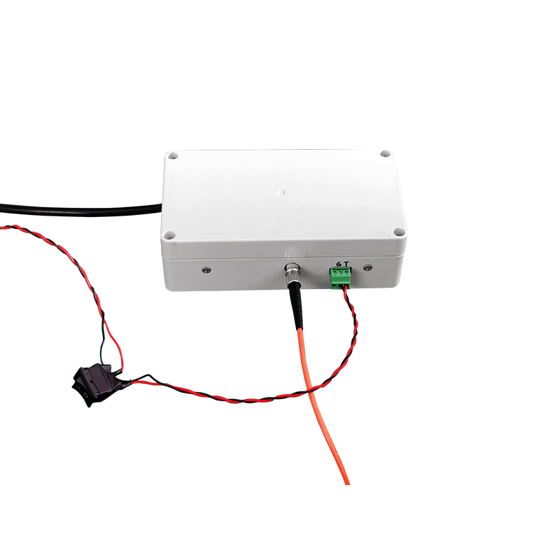
Application and Optimization of High-Voltage Power Supplies in Laser Marking
In the laser marking technology system, high-voltage power supplies (HVPS) serve as core components for laser energy regulation. Their output characteristics directly determine the peak power, pulse stability, and energy uniformity of laser beams, thereby influencing marking precision, efficiency, and material adaptability. By precisely controlling high-voltage electric field parameters, HVPS enable fine-tuning of laser pulse waveforms, repetition frequency, and energy density, providing differentiated solutions for surface marking on metal, non-metal, and composite materials. This article explores the key application scenarios and optimization strategies of HVPS in laser marking from a technical and engineering perspective.
1. Core Functions of HVPS in Laser Marking Systems
Laser marking relies on pulsed lasers to generate high-energy-density beams that form permanent marks on material surfaces through ablation, melting, or color-changing effects. HVPS perform two critical technical roles:
1. Pulsed Laser Drive: For solid-state pulsed lasers (e.g., Nd:YAG, fiber lasers), HVPS provide instantaneous high-voltage excitation for pumping modules (e.g., xenon lamps, semiconductor laser diodes), inducing population inversion in the working medium. Take Nd:YAG lasers as an example: a high-voltage pulse power supply generates 5-20kV trigger voltage, combined with an energy storage capacitor bank to achieve nanosecond-level pulse width output with megawatt-level peak power.
2. Electro-Optic Modulation Control: In CO₂ gas lasers or all-solid-state lasers, HVPS drive electro-optic modulators (e.g., Pockels cells) by applying kilovolt-level alternating voltages to adjust the refractive index of crystals, enabling fast switching and pulse waveform shaping of laser beams. The rise time of the modulation voltage (required to be <5ns) and voltage stability (ripple ≤0.1%) directly affect the edge clarity of marked lines.
2. Typical Application Scenarios and Technical Requirements
1. Energy Uniformity Optimization for Precision Marking on Metal Materials
When marking stainless steel, aluminum alloy, and other metal surfaces, it is necessary to avoid excessive ablation or blurring caused by local overheating. HVPS dynamically adjust the energy distribution of pulse sequences to achieve:
Adaptive Waveform Parameters: For different metal reflectivities (e.g., copper >80%), the power supply supports continuous adjustment of pulse width (0.1-100μs) and repetition frequency (1-100kHz), ensuring surface micro-melting while reducing heat diffusion.
Energy Closed-Loop Control: Integrated with high-voltage sensors and feedback algorithms, it real-time monitors the output energy of the laser head. By adjusting the charging voltage (typical range 0-3kV), energy fluctuations are controlled within ±2%, ensuring consistent marking depth at all points in complex patterns.
2. Frequency Response Enhancement for High-Speed Marking on Non-Metal Materials
Non-metal materials such as plastics and ceramics are sensitive to laser pulse frequency. High-frequency marking (>50kHz) reduces single-pulse energy to avoid material breakdown. HVPS need to have:
Nanosecond-Level Edge Response: Using all-solid-state switching devices (e.g., IGBT series modules), the pulse rise time is compressed to <20ns. With an internal LC matching network, low-distortion output is achieved at high frequencies.
Multi-Channel Synchronous Triggering: In large-format marking systems, the digital trigger interface (e.g., differential signal synchronization) of HVPS precisely controls the collaborative operation of multiple lasers, ensuring no misalignment in stitched areas with a positional accuracy of ≤±5μm.
3. Waveform Customization for Composite Material Marking
For multi-layer coated materials or flexible substrates, HVPS generate special waveforms (e.g., dual-peak pulses, step voltages) for hierarchical processing:
Pre-Ionization Pulse Design: A microsecond-level low-voltage pre-ionization pulse (e.g., 500V) is applied before the main pulse, reducing the threshold energy of the material surface and increasing the energy utilization rate of the subsequent main pulse (1.5kV) by 30%, while minimizing substrate thermal stress.
Energy Gradient Output: Using an internal digital signal processor (DSP), the power supply generates pulse sequences with exponentially decaying voltage amplitudes, achieving a transition effect from deep to shallow at the mark edges to meet high-precision graphic marking requirements.
3. Optimization Directions and Key Technologies for HVPS
1. High-Frequency and Miniaturized Design
Traditional HVPS issues such as large volume (≥20L) and low efficiency (<70%) have been improved through:
Wide-Bandgap Semiconductor Application: Replacing traditional silicon-based devices with SiC MOSFETs increases the switching frequency to >100kHz. Combined with planar transformer technology, the power density of the power supply is increased from 1kW/L to 5kW/L.
Soft Switching Technology: Zero-voltage switching (ZVS) or zero-current switching (ZCS) topologies reduce switching losses by 40% and suppress electromagnetic interference (EMI), ensuring control circuits are unaffected by power supply noise during marking.
2. Intelligent Control and Fault Diagnosis
Adaptive Algorithm Integration: A built-in material database automatically matches optimal voltage waveforms, pulse widths, and frequency parameters based on the input material type (metal/non-metal/composite), reducing manual debugging time by over 50%.
Condition Monitoring System: Using high-voltage voltage-dividing resistors (accuracy 0.05%) and temperature sensors, it real-time monitors the internal insulation performance and heat dissipation status of the power supply. When abnormal discharge (e.g., partial discharge >10pC) is detected, it automatically triggers protective shutdown to avoid laser damage.
3. Energy Efficiency Improvement and Thermal Management Optimization
Energy Recovery Technology: During pulse intervals, residual energy in the energy storage capacitor is fed back to the power grid through a flyback circuit, increasing power supply efficiency from 75% to >85% and reducing energy costs for industrial marking equipment.
Liquid Cooling Structure: Combining micro-channel liquid-cooled plates (channel size ≤0.5mm) with phase-change materials keeps the junction temperature of power modules below 85℃, ensuring stability during 24-hour continuous marking.
4. Future Development Trends
With the popularization of new technologies such as ultraviolet laser marking and femtosecond laser microprocessing, HVPS will evolve toward:
1. Ultra-High-Speed Response: Developing high-voltage pulse power supplies with sub-nanosecond rise times to meet the synchronous triggering requirements of femtosecond lasers for micro-scale structure processing.
2. Multi-Dimensional Regulation: Integrating three-dimensional control of voltage, current, and phase to support elliptically polarized laser output and expand marking capabilities for complex structures such as curved surfaces and deep holes.
3. Green Design: Adopting capacitor-free architectures and efficient EMC designs to reduce hazardous substance use, aligning with the environmental manufacturing requirements of Industry 4.0.