Research and Application Progress in Low-Ripple Optimization of High-Voltage Power Supplies for Electron Microscopes
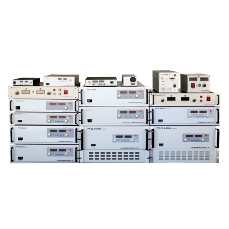
Ripple control in high-voltage power supplies is a core performance indicator for transmission electron microscopes (TEMs). Ripple (periodic fluctuations in output voltage) directly affects the stability of the electron beam, leading to reduced image resolution and contrast distortion. Recently, with breakthroughs in domestic TEM production in China, low-ripple optimization of high-voltage power supplies has become a key technological focus, with significant implications for materials science, life sciences, and the semiconductor industry.
I. Technical Pathways for Low-Ripple Optimization
Stability Design for Electron Gun Power Systems
Field-emission electron guns are highly sensitive to power supply ripple. Excessive ripple reduces electron emission stability and degrades image coherence. Optimization strategies include:
High-Stability, Low-Ripple High-Voltage Power Supplies: Active compensation techniques (e.g., current/voltage injection) counteract ripple via feedback loops.
Electromagnetic Lens System Matching: Electron optical designs optimized for high-voltage platforms (e.g., 120kV) minimize interference from power fluctuations.
Multi-Stage Filtering and Topology Innovations
Hybrid Filtering: Combining LC filters (suppressing high-frequency ripple) with active compensation circuits (reducing low-frequency ripple) achieves ripple coefficients below 0.01%.
Switching Topology Improvements: In Buck-Boost circuits, increasing output inductance ( \Delta I \propto 1/L ) and capacitance ( \Delta V \propto 1/C ) significantly attenuates high-frequency ripple (Table 2).
Digital Compensation and Intelligent Control
Adaptive Ripple Compensation: Digital signal processors (DSPs) analyze ripple spectra in real time, dynamically adjusting parameters to adapt to load changes.
Harmonic Injection: Injecting phase-inverted harmonics into control loops cancels switching noise (e.g., 50MHz–100MHz spikes).
II. Ripple Measurement and Performance Evaluation
Accurate measurement is essential for optimization:
Oscilloscope Testing:
Utilizes 20MHz bandwidth limitation, AC coupling, and ground springs to shorten probe leads and avoid electromagnetic interference.
Key Metrics:
Ripple rejection ratio (input/output ripple amplitude ratio), phase margin (>45° for stability), and temperature drift coefficient (<50ppm/℃).
III. Application Challenges and Future Directions
Extreme Condition Adaptation
Under low-electron-dose imaging, power supplies must maintain μV-level ripple at microampere currents, requiring ultra-low capacitor ESR (<10mΩ).
Integration and Thermal Management
Miniaturization necessitates thermal solutions. SiC/GaN wide-bandgap semiconductors reduce switching losses but require optimized PCB layouts:
Minimized power loops;
Feedback routing away from noise sources.
Next-Generation Technologies
For 200kV+ platforms, multi-stage ripple compensation architectures integrating feedforward control and AI algorithms will enable nanovolt-level suppression.
Conclusion
Low-ripple optimization of high-voltage power supplies underpins the domestic advancement of TEMs. Through interdisciplinary integration (power electronics, materials science, control theory), China has transitioned from 100% import dependence to atomic-resolution imaging. Future developments in digital compensation and wide-bandgap semiconductors will support higher-voltage, higher-resolution microscopes, providing an ultra-stable foundation for cutting-edge research.
