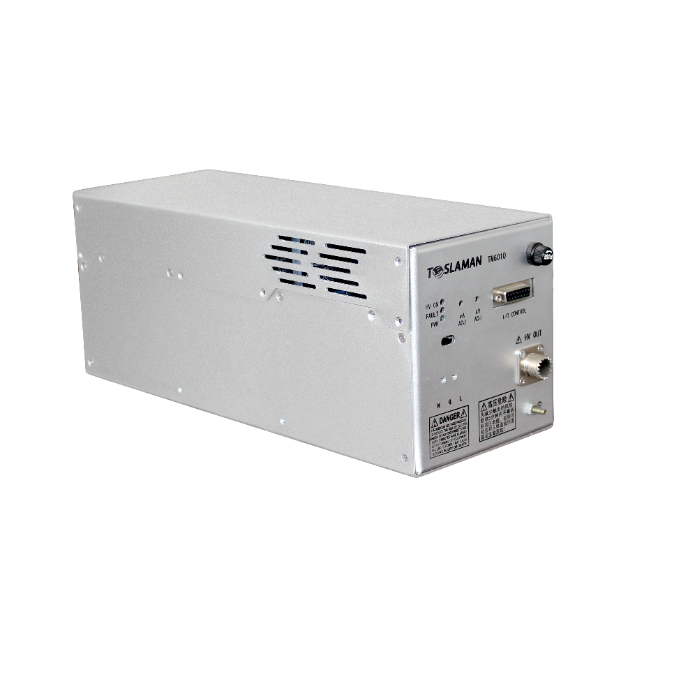
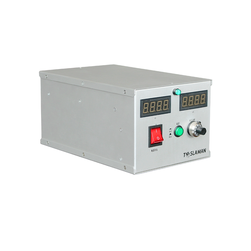
Multidimensional Pathways and Technological Evolution in Efficiency Optimization of Ion Implantation High-Voltage Power Supplies
Ion implantation technology is a core process in semiconductor manufacturing, where its precision directly determines the electrical characteristics and reliability of devices. As the power heart of ion implantation systems, the efficiency optimization of high-voltage power supplies has become pivotal for pushing the limits of semiconductor manufacturing. This article explores the technical pathways and trends in efficiency optimization from multiple dimensions: material innovation, control strategies, thermal management, and system design.
1. Revolution in Power Device Materials: Application of Wide-Bandgap Semiconductors
Traditional silicon-based power devices face limitations in conduction resistance and switching losses, constraining the efficiency of high-voltage power supplies. Third-generation semiconductor materials such as silicon carbide (SiC) and gallium nitride (GaN) have emerged as breakthroughs due to their high critical breakdown field strength, low conduction resistance, and high-frequency characteristics:
• Switching Frequency Enhancement: SiC/GaN devices operate at frequencies exceeding hundreds of kHz, three times higher than traditional silicon devices, reducing the size and losses of magnetic components.
• Reduced Conduction Losses: Experiments show that SiC MOSFETs reduce conduction resistance by over 38%, boosting overall power supply efficiency beyond 94% when combined with low-loss magnetic cores (e.g., soft magnetic composites).
• High-Temperature Stability: Wide-bandgap semiconductors withstand temperatures above 200°C, adapting to high-temperature ion implantation chambers and minimizing cooling energy consumption.
2. Control Strategy Upgrade: Digitalization and Intelligent Synergy
Dynamic voltage accuracy and response speed directly impact the uniformity of impurity distribution during ion implantation. Digital control achieves precision energy delivery through multi-stage closed-loop feedback and intelligent algorithms:
• High-Precision Voltage Regulation: Digital Pulse Width Modulation (DPWM) combined with closed-loop feedback suppresses output voltage ripple to below 0.01%, ensuring impurity concentration deviation ≤ ±2%.
• Millisecond Dynamic Response: AI-driven parameter optimization systems monitor ion source fluctuations and vacuum changes in real-time, adaptively adjusting acceleration voltage and beam current within milliseconds to maintain process stability.
• Space Charge Effect Mitigation: Electric field distribution algorithms neutralize beam divergence in low-energy, high-current ion beams, increasing transmission efficiency by over 30%.
3. Thermal Management Breakthrough: Efficient Cooling and Compact Design
Increasing power density demands advanced thermal solutions to prevent efficiency degradation due to overheating:
• Microchannel Liquid Cooling: Embedded microchannel heat sinks improve thermal conductivity by 50% compared to traditional air cooling, supporting power densities up to 5 kW/L while reducing volume by 40%.
• Topology Optimization: Architectures like CLLC resonant converters and phase-shifted full-bridge reduce switching losses through soft-switching techniques (ZVS/ZCS), minimizing heat generation.
4. System-Level Optimization: Integrated Design and Reliability Assurance
Efficiency optimization requires balancing electrical performance with system robustness:
• Multi-Module Integration: Functional units (e.g., acceleration tubes, quadrupole lens power supplies, deflection power supplies) are highly integrated. Graded focusing compresses beam spot size (e.g., adjusting Q1/Q2 lens currents), reducing transmission losses.
• Arc Suppression and Redundancy: Magnetically isolated drivers and nanosecond transient detection circuits cut off energy during high-voltage breakdown, reducing failure rates to <0.1 incidents per thousand hours. Multi-level protection (overvoltage/overcurrent/overtemperature) ensures long-term operation in complex electromagnetic environments.
Conclusion: Convergence of Technologies for Efficiency Optimization
Efficiency optimization in ion implantation high-voltage power supplies has evolved from component-level upgrades to deep integration of materials, control, thermodynamics, and system design: wide-bandgap semiconductors lay the foundation, digital control enables atomic-scale precision, advanced cooling overcomes physical limits, and system integration ensures reliability. Moving forward, edge computing and digital twin technologies will dynamically synchronize power efficiency with process parameters, propelling semiconductor manufacturing toward a zero-defect era.