Multi-Stage Voltage Regulation Scheme for High-Voltage Power Supplies in Lithography Machines
As the core equipment of semiconductor manufacturing, lithography machines determine the nanoscale structure of chips. In lithography processes, high-voltage power supplies drive deep ultraviolet (DUV) or extreme ultraviolet (EUV) light sources, where voltage stability directly impacts pattern transfer accuracy. For instance, millivolt-level fluctuations in source power may cause exposure dose deviations, leading to chip layer thickness errors or pattern distortion. Thus, a multi-stage voltage regulation scheme is essential to achieve precise control from kilovolt-level inputs to millivolt-level ripple.
1. Technical Architecture of Multi-Stage Regulation
The scheme typically comprises four stages:
• Input Filtering Stage: Multi-level EMI filters suppress grid high-frequency noise to μV levels, providing clean AC power.
• Rectification & PFC Stage: A three-phase totem-pole PFC (Power Factor Correction) architecture with silicon carbide (SiC) devices boosts efficiency (e.g., 96.5% peak efficiency in 11kW modules) and adjusts output voltage (500-900Vdc), while maintaining power factor >0.99.
• High-Voltage DC Generation: LLC resonant or phase-shifted full-bridge topologies convert high-voltage DC to multi-channel low-voltage outputs (e.g., ±12V, ±5V). Zero-voltage switching (ZVS) reduces switching losses by 40% and limits ripple to ≤±0.1% at 200A.
• Precision Regulation Stage: Hybrid linear-digital control with optocoupler isolation monitors output. PID algorithms dynamically adjust PWM duty cycles, achieving <1ms transient response during load突变 (e.g., wafer stage movement).
2. Key Challenges and Solutions
• Nanoscale Ripple Suppression: Servo motors require ±5nm positioning accuracy, demanding output fluctuations ≤±0.1%. Solutions include:
• Dynamic load compensation algorithms for real-time current adjustment;
• Dual-redundancy architecture with <10ms failover.
• High-Voltage Isolation & Safety: Reinforced insulation (e.g., IEC 60950) is achieved through:
• Optocoupler-isolated feedback to block common-mode noise;
• 1,200V-rated SiC devices;
• Overvoltage clamping circuits to limit inrush stress.
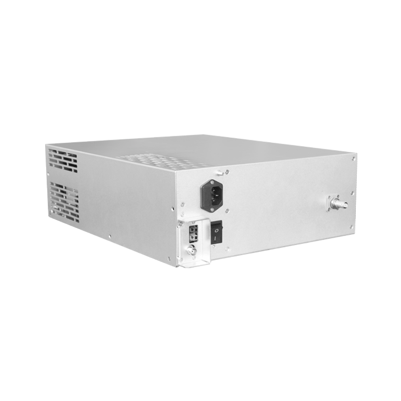
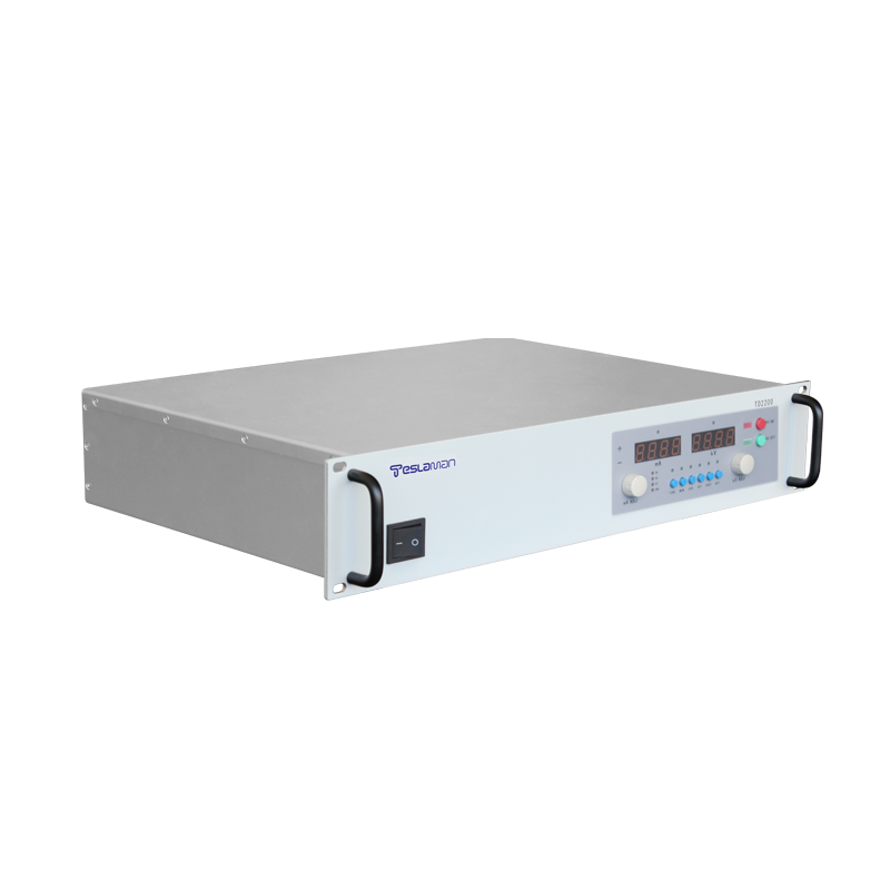
• Thermal Management & Space Optimization: A 2U compact design maintains ≤70℃ hotspot temperature under 80℃ ambient using distributed cooling (heat pipes + forced convection), with power density reaching 4kW/U.
3. System Integration and Validation
Reliability is verified through:
• EMC Performance: Conducted (CE) and radiated emissions (RE) surpassing CISPR35 Class A;
• Robustness Validation: 100G vibration tests (MIL-STD-810H) and -40℃~+100℃ thermal cycling ensure 100,000-hour MTBF;
• Closed-Loop Control: An ARM Cortex-M7 MCU (300MHz) with dedicated M0 core for HSM safety enables real-time diagnostics and OTA updates.
4. Conclusion: Balancing Precision and Reliability
This multi-stage scheme represents an optimal trade-off among efficiency, accuracy, space, and reliability. Future trends will focus on:
• AI-driven adaptive regulation for load prediction;
• SiC/GaN integrated designs to enhance power density;
• Full-system simulation to preempt coupling effects between power and lithography systems.
Multi-stage regulation is not merely an engineering feat but a cornerstone sustaining Moore’s Law—each millivolt of stability paves the way for atomic-scale precision as lithography advances into the ångstrom era.