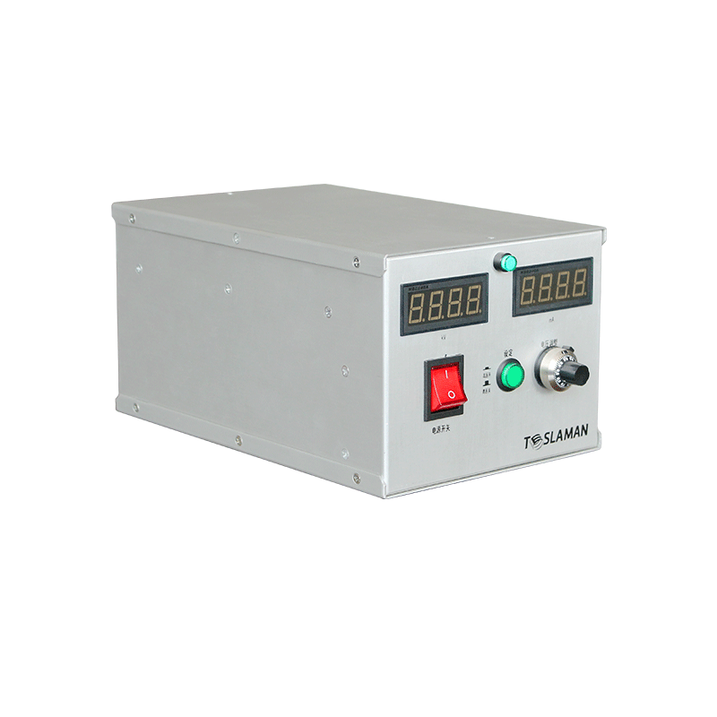
High-Frequency Oscillation Suppression Technology in High-Voltage Power Supplies for Electrostatic Chucks
Electrostatic chucks, a core component in semiconductor manufacturing, rely on high-voltage power supplies to generate electrostatic fields for non-contact fixation of wafers. However, high-frequency oscillation in high-voltage power supplies—often triggered by switching noise, parasitic parameter resonance, or temperature drift—can cause output voltage fluctuations, leading to unstable wafer clamping force and potential wafer displacement or micro-damage. Recent advancements in oscillation suppression technologies have significantly enhanced the precision and reliability of electrostatic chucks.
1. Causes and Impacts of High-Frequency Oscillation
High-voltage power supplies for electrostatic chucks must deliver precise voltages (e.g., ±2500V) within milliseconds and switch polarity within seconds. Oscillation risks arise from:
1. Switching Noise and Parasitic Parameters: Switching actions of power devices (e.g., IGBT) resonate with parasitic capacitances/inductances, generating MHz-level oscillations.
2. Temperature Drift: A 10°C ambient temperature fluctuation causes a 0.15% output voltage drift in conventional power supplies, increasing local wafer detachment risk by 42%.
3. Dynamic Load Variations: Gas dielectric constant shifts in vacuum chambers (Δε/ΔT≈0.05%/℃) induce capacitive load mismatch, amplifying oscillations.
2. Core Oscillation Suppression Technologies
2.1 Temperature Compensation for Voltage Reference
Second-order curvature compensation combines PTAT (positive temperature coefficient) and CTAT (negative temperature coefficient) currents to reduce the temperature coefficient from 35 ppm/℃ to 3 ppm/℃. This limits reference voltage drift to <0.005% within 25–100°C, suppressing temperature-induced oscillations at the source.
2.2 Thermal Stability Optimization for Power Devices
• Low-Thermal-Resistance Devices: Wide-bandgap semiconductors (e.g., GaN) replace silicon-based IGBTs, reducing thermal resistance by 60%. Coupled with real-time thermistor feedback, this maintains power efficiency >92% and limits temperature rise to ΔT<15°C.
• Conduction Resistance Drift Control: A 50°C junction temperature increase triples output voltage ripple. Optimized heat dissipation and driving logic reduce ripple amplitude to one-third of its original value.
2.3 Dynamic Load Matching Technology
To address load mismatch from dielectric constant variations:
• FPGA-Controlled LC Resonance Networks: Monitor load phase angles (±0.1° accuracy) and dynamically adjust resonance frequency within 200μs, reducing clamping force fluctuation from ±5% to ±0.8%.
• Impedance Adaptive Algorithms: Automatically optimize LC parameters based on real-time wafer permittivity and chamber pressure data.
2.4 System-Level Multi-Physics Field Coupling
• DC Self-Bias Voltage Superposition: Integrates plasma sheath voltage (potential difference between wafer and plasma) into the high-voltage output. This compensates for process chamber bias fluctuations caused by RF power instability.
• Digital Twin Prediction Models: Predict oscillation risks using real-time temperature, load current, and dielectric constant data, compressing temperature drift coefficients to 0.5 ppm/℃.
3. Future Technological Trends
Next-generation oscillation suppression will focus on:
1. Integration of Wide-Bandgap Semiconductors and Edge Computing: Leveraging the low switching losses of SiC/GaN devices with edge computing chips for nanosecond-level oscillation detection and suppression.
2. Multimodal Sensor Feedback: Closed-loop control systems incorporating temperature, permittivity, and clamping force sensors enable temperature-agnostic nano-level wafer positioning.
Conclusion
High-frequency oscillation suppression technologies—through synergistic innovations in device compensation, circuit matching, and system control—have dramatically improved the stability of high-voltage power supplies for electrostatic chucks. As semiconductor processes advance toward sub-3nm nodes, these technologies will play a pivotal role in wafer yield control and process repeatability, marking a critical breakthrough in high-end manufacturing equipment autonomy.