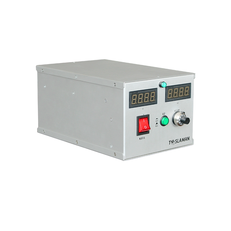
Modular Design of High-Voltage Power Supplies for Exposure Machines: Technological Advances and Applications
As the core equipment in semiconductor manufacturing, exposure machines determine the linewidth and yield of chips through pattern transfer precision. The high-voltage power supply, serving as the energy heart of these machines, must generate stable, low-noise high-voltage electric fields for electron or ion beam generation systems. Modular design has significantly enhanced power supply reliability, maintenance efficiency, and system integration through architectural innovation, becoming a critical pathway for modern exposure machine advancements.
1. Core Advantages of Modular Design
Enhanced System Reliability
Traditional centralized high-voltage power supplies carry single-point failure risks. Modular designs adopt a distributed architecture, decomposing high-voltage generation, control logic, and protection circuits into independent submodules. Each module features redundant backup capabilities; if one module fails, the system automatically switches to a backup unit, ensuring continuous exposure processes. For example, during wafer exposure, power output stability (ripple coefficient <0.01%) directly impacts pattern edge definition. Modular designs suppress current fluctuations through multi-channel parallel current-sharing technology, reducing defect rates.
Optimized Thermal Management
High-voltage power conversion often generates localized hotspots, accelerating component aging. Modular designs employ three-dimensional thermal layouts that separate power units from control units: power units dissipate heat via metal substrates, while control units use internal air ducts for forced convection. Tests show this design reduces temperature rise by 15°C at full load and extends service life by over 20%.
Reduced Maintenance Costs
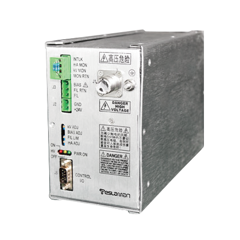
Exposure machines operate in cleanroom environments where traditional power supply failures require full disassembly. Modular units support hot-swapping, cutting maintenance time from 72 hours to 2 hours. Additionally, real-time health monitoring through digital interfaces (e.g., RS-485, Ethernet) enables predictive maintenance, decreasing downtime probability by 40%.
2. Key Technical Implementation Approaches
Integrated Power Topology
Zero-voltage switching (ZVS) and multi-phase interleaving techniques resolve the efficiency-volume trade-off. By integrating boost transformers, rectifiers, and filtering networks onto a single ceramic substrate, power density triples while achieving miniaturization (typical size <30×100×120mm) under high outputs (e.g., 60kV/10A).
Adaptive Control Strategy
An FPGA-based closed-loop system dynamically compensates for load variations:
• Voltage Adaptation: Real-time gain adjustment ensures ±0.005% stability;
• Ripple Cancellation: Phase-shift superposition suppresses high-frequency ripple below 0.05%, eliminating periodic pattern distortion.
High Isolation and Noise Immunity
Complex electromagnetic environments in exposure machines demand triple isolation:
• Electrical Isolation: 6kVDC withstand voltage blocks ground loop interference;
• Magnetic Shielding: μ-metal layers suppress magnetic coupling;
• Digital Filtering: Kalman filtering improves ADC signal-to-noise ratio by 30dB.
3. Future Prospects and Challenges
As advanced nodes like GAA transistors proliferate, exposure machines require higher voltages (>100kV) and faster response (<10ms rise time). Modular designs enable flexible voltage scaling through stackable expansion. However, nanoscale exposure introduces new challenges:
• Quantum Noise Suppression: Random tunneling noise becomes significant at ppm-level voltage precision;
• Material Limitations: Wide-bandgap semiconductors (SiC/GaN) face avalanche breakdown risks above 150kV. Future innovations may explore diamond-based power devices combined with topology optimization algorithms.
Modular high-voltage power supplies are redefining the performance boundaries of exposure machines. Their value extends beyond improving individual specifications—standardized interfaces foster collaborative upgrades across semiconductor equipment chains, forming an evolvable technological ecosystem that underpins the lithography revolution in the sub-nanometer era.