Research on Load Adaptability of Electron Beam High-Voltage Power Supplies
Electron beam processing technologies (such as welding, cutting, heat treatment, and additive manufacturing) rely critically on the load adaptability of high-voltage power supplies. The processing targets span diverse materials including metals, semiconductors, and ceramics, whose load characteristics (e.g., impedance, heat capacity, conductivity) vary significantly. This demands dynamic response, wide-range adjustability, and multi-parameter coordination from the power supply. Load adaptability directly determines processing precision, energy efficiency, and equipment reliability. Research in this field must address three dimensions: load characterization, dynamic response mechanisms, and multi-system integration.
1. Load Characteristics and Adaptation Challenges
Electron beam processing loads exhibit three key traits:
1. High Dynamic Range: Physical changes like material evaporation or melting cause load impedance to fluctuate drastically (e.g., from MΩ to kΩ in microseconds), requiring output voltage (60–300 kV) and current (μA to 50 A) stability within 0.1%.
2. Multi-Parameter Coupling: The main high-voltage supply must coordinate with filament (≤50 A) and grid bias (≤3000 V) supplies. Filament current fluctuations affect electron emission density, necessitating closed-loop control across all power modules.
3. Nonlinear Thermal Effects: Continuous high-power operation (e.g., 500 kW electron beam melting) induces thermal drift in material resistivity, requiring real-time compensation to maintain energy density uniformity.
2. Core Technologies for Load Adaptation
Modern power supplies employ these strategies:
1. Multi-Stage Feedback Control
• Voltage-Current Dual Loop: An inner loop adjusts switching frequency (0.1 Hz–1 MHz) to suppress transients, while an outer PID loop maintains output ripple <0.3% (RMS) for precise beam focusing.
• Adaptive Tuning: Dynamically adjusts LC resonance parameters (e.g., zero-voltage full-bridge topology) to achieve ±0.01% load regulation across conditions from no-load to short-circuit.
2. Intelligent Algorithms for Dynamic Response
• Dynamic Load Tracking Algorithm (DLTA): Predicts step changes (e.g., beam start/stop), reserves 30% power redundancy, and reduces response time to milliseconds to prevent processing defects.
• Temperature-Power Coupling Model: Integrates thermal sensors to derate output (e.g., 10% current reduction at 125°C) based on ambient temperature (-20–40°C), avoiding false triggering of protection circuits.
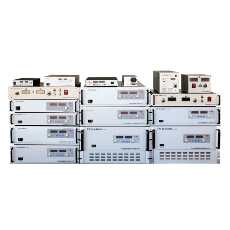
3. Modular and Integrated Design
• Unified Multi-Supply System: Integrates main high-voltage, filament, and grid bias supplies with digital interfaces (RS232/USB/Ethernet) to synchronize parameters, reducing energy loss and achieving ≥95% system efficiency.
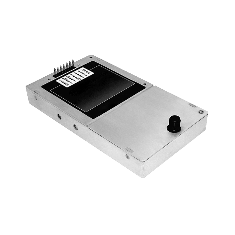
• Air-Insulated Compact Design: Replaces traditional potting with air insulation, lowering thermal resistance (Rθjc <3°C/W) and enabling 1U rack deployment for space-constrained applications.
3. Application Validation and Future Trends
In electron beam additive manufacturing, load adaptation improves inter-layer fusion consistency to 99.5%. For semiconductor lithography, nano-scale beam stability achieves ±2 nm linewidth precision. Future research will focus on:
• Wide-Bandgap Semiconductors: Using SiC/GaN devices to increase switching frequency (>1 MHz) and extend voltage range (0–500 kV).
• Digital Twin Pre-Adaptation: Simulating load characteristics to pre-configure power parameters, reducing commissioning time by 50%.


