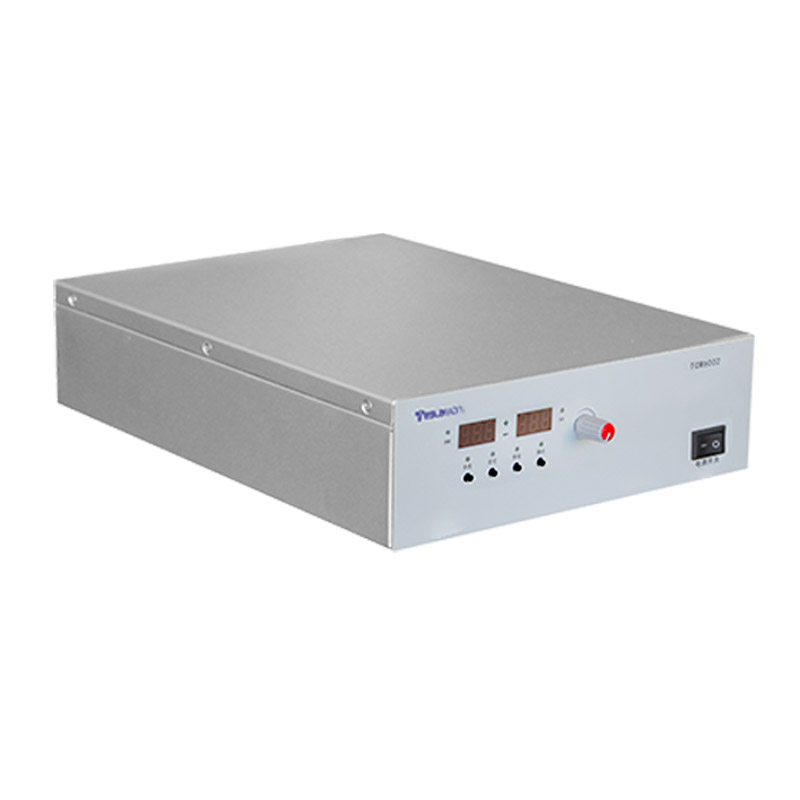
Wide-Range Voltage Regulation Techniques for Adjustable Voltage Power Supplies
Adjustable voltage power supplies (usually covering an output voltage range of 0~rated voltage or a wider input and output range) are widely used in laboratory testing, industrial equipment power supply and other scenarios. Their wide-range voltage regulation performance directly affects the adaptability and testing accuracy of the equipment. To achieve wide-range voltage regulation, it is necessary to break through technical bottlenecks from four aspects: topological structure selection, control algorithm optimization, component selection, and ripple suppression, to ensure stable output, high accuracy, and low loss in the full voltage regulation range.
The selection of topological structure is the basis for realizing wide-range voltage regulation. Different voltage regulation ranges have different requirements for topological structures, and appropriate topologies should be selected according to actual needs: for scenarios with a wide input voltage range (such as AC 85~265V) and a narrow output voltage range (such as DC 12~24V), the Buck-Boost topology is adopted. This topology realizes voltage regulation when the input voltage is higher or lower than the output voltage through inductor energy storage, and has a simple structure and low cost. For scenarios with a narrow input voltage range and a wide output voltage range (such as DC 24~100V), the full-bridge phase-shifted topology is adopted. By adjusting the phase shift angle of the switching tubes, the continuous adjustment of the output voltage is realized, the voltage regulation range can reach 1:4, and the conversion efficiency is high (93% at rated load). For scenarios with both wide input and output voltage ranges (such as AC 85~265V input and DC 5~100V output), the "PFC + DC/DC" combined topology is adopted: the front-stage PFC (Power Factor Correction) circuit adopts the Boost topology to stabilize the input voltage to DC 400V, and the rear-stage DC/DC circuit adopts the LLC resonant topology to realize wide-range output by adjusting the resonant frequency. The combined topology has a voltage regulation range of up to 1:20, and the power factor is above 0.98, meeting the requirements of energy efficiency standards. In addition, for ultra-wide output voltage scenarios (such as DC 0.1~500V), a modular topology is adopted, dividing the output into three modules: low-voltage segment (0.1~50V), medium-voltage segment (50~200V), and high-voltage segment (200~500V). The modules are switched through relays to realize full-range voltage regulation. Each module adopts the optimal topology to ensure the efficiency and accuracy of each voltage segment.
The optimization of control algorithm improves the accuracy and dynamic response of wide-range voltage regulation. The traditional linear control algorithm (such as PID) is prone to parameter mismatch problems (such as slow response in the low-voltage segment and large overshoot in the high-voltage segment) during wide-range voltage regulation, leading to unstable output. The optimized scheme combines segmented control and adaptive algorithm: first, divide the output voltage range into multiple intervals (such as each 50V as an interval), determine the optimal PID parameters for each interval through simulation and experiment, store them in the controller, and automatically call the corresponding parameters according to the current output voltage during voltage regulation. Second, introduce the Model Predictive Control (MPC) algorithm, establish a mathematical model of the power supply (considering the dynamic characteristics of inductors and capacitors), predict the output voltage at future moments, and adjust the control quantity in advance, so that the dynamic response time is shortened to 30μs and the overshoot is controlled within 2%. In addition, in view of the load change during voltage regulation, current feedforward control is adopted to compensate the influence of load current on the output voltage in real time, so that the load regulation rate (from no-load to full-load) is controlled within 0.5%, ensuring the voltage regulation accuracy.
Component selection adapts to the needs of wide-range voltage regulation. The parameter characteristics of components directly affect the voltage regulation range and performance: in the selection of power semiconductor devices, for wide input voltage scenarios, high-voltage-resistant devices are selected (such as IGBTs with a voltage resistance level of 1200V) to avoid device breakdown caused by excessive input voltage; for wide output voltage scenarios, MOSFETs with low on-resistance are selected (such as on-resistance ≤5mΩ) to reduce conduction loss during high-voltage output. In the selection of inductors and capacitors, inductors should have wide current range characteristics (such as the saturation current is 1.5 times the rated current) to avoid inductor saturation during low-voltage and high-current output; capacitors use electrolytic capacitors or film capacitors with low ESR (Equivalent Series Resistance) to reduce ripple and loss. In addition, for ultra-low voltage output scenarios (such as DC 0.1~5V), a precision operational amplifier (such as offset voltage ≤10μV) is used to form a feedback circuit to improve the voltage sampling accuracy; for ultra-high voltage output scenarios (such as DC 500~1000V), high-voltage voltage divider resistors (such as 100MΩ high-precision resistors) are used for voltage sampling to ensure the sampling error ≤0.1%.
Ripple suppression ensures the output quality of wide-range voltage regulation. During wide-range voltage regulation, due to factors such as switching frequency change and load fluctuation, the output ripple is easy to increase, affecting the normal operation of the equipment. Ripple suppression needs to be carried out from both filter circuit and control strategy: in the design of the filter circuit, a multi-stage filter structure is adopted, the front stage is a differential-mode inductor and X capacitor to suppress differential-mode ripple; the rear stage is a common-mode inductor and Y capacitor to suppress common-mode ripple; for low-voltage output scenarios, an LC filter is added (inductor value ≥100μH, capacitor value ≥1000μF) to control the ripple voltage within 5mV; for high-voltage output scenarios, a combination of high-voltage film capacitors (such as 10μF/1000V) and high-frequency inductors is used to control the ripple voltage within 50mV. In terms of control strategy, frequency dithering technology is adopted to dither the switching frequency within the range of ±5kHz, disperse the ripple energy, and reduce the ripple peak at a specific frequency; at the same time, digital filtering algorithms (such as Kalman filtering) are used to process the sampled voltage to reduce noise interference and further reduce ripple.
Through the above wide-range voltage regulation techniques, the adjustable voltage power supply can achieve an ultra-wide output range of 0.1V~1000V, with a voltage regulation accuracy of ±0.1%, an output ripple ≤50mV, and a dynamic response time ≤50μs, meeting the needs of complex scenarios such as laboratory precision testing and industrial multi-equipment power supply.