Electron Beam Focus Optimization of High-Voltage Power Supplies for Scanning Electron Microscopes
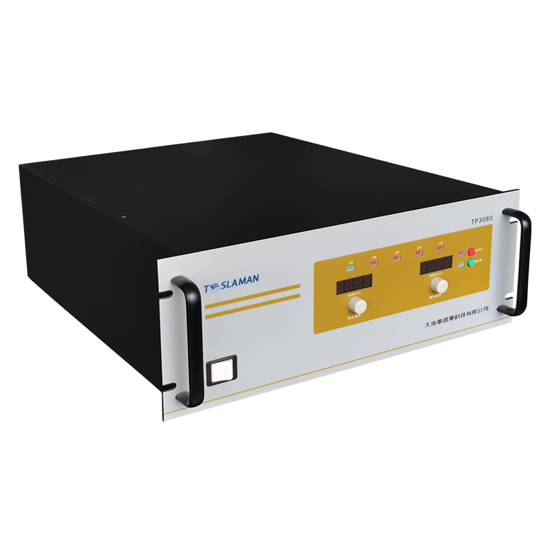
Scanning Electron Microscopes (SEM) are widely used in the microstructural analysis of materials science, biomedicine and other fields due to their high-resolution imaging capabilities. The quality of electron beam focusing directly determines the imaging resolution of SEM - the smaller the focused spot, the higher the resolution. The electron beam focusing of SEM relies on the accelerating voltage and beam current control provided by the high-voltage power supply (HVPS). The current HVPS has problems such as unstable accelerating voltage and low beam current modulation accuracy, which lead to electron beam energy fluctuation and focused spot diffusion, affecting imaging quality. Therefore, the electron beam focusing optimization of SEM HVPS needs to start from three aspects: voltage stability control, beam current precise modulation, and coordinated control strategy.
In terms of accelerating voltage stability control, a three-stage architecture of "reference voltage source + error amplification + power adjustment" is adopted: the reference voltage source uses a high-precision bandgap reference, with the temperature coefficient controlled within 5ppm/℃ to ensure stable reference voltage; the error amplification link uses a high-gain operational amplifier to amplify the voltage error by 1000 times, realizing accurate capture of small errors; the power adjustment link uses a push-pull power amplifier circuit, combined with negative feedback control, to improve the accelerating voltage stability to ±0.005%, reducing the electron beam energy change caused by voltage fluctuation.
In the precise beam current modulation, a beam current control circuit based on Metal-Oxide-Semiconductor Field-Effect Transistor (MOSFET) is designed: the beam current is accurately adjusted by changing the gate voltage of the MOSFET, the beam current adjustment range is 10pA-100nA, and the adjustment accuracy reaches ±0.1pA. At the same time, a beam current feedback monitoring module is introduced, and a Faraday cup is used to collect beam current data in real time. When the beam current deviation exceeds 0.5%, the gate voltage of the MOSFET is automatically adjusted to realize the closed-loop control of the beam current and ensure the stable intensity of the electron beam.
In terms of the coordinated control strategy, a linkage mechanism between HVPS and the SEM deflection system is established: data interaction between the two is realized through a high-speed serial port. When the deflection system adjusts the electron beam scanning trajectory, HVPS synchronously adjusts the accelerating voltage and beam current parameters to ensure that the electron beam can be accurately focused at different scanning positions. In addition, a thermal management system is designed, which adopts a combined heat dissipation method of liquid cooling and air cooling to control the internal temperature of HVPS at 25±1℃, avoiding the parameter drift of electronic components caused by temperature changes and further improving the output stability.
After the application of this optimization scheme in the SEM of a scientific research institution, the imaging resolution was increased from 10nm to 5nm, the diameter of the focused spot was reduced to 8nm, and the detail display of the material microstructure was clearer, providing higher-precision equipment support for scientific research in the microcosmic field.