Simultaneous Improvement of Capacity and Efficiency in CMP Equipment Power Supplies
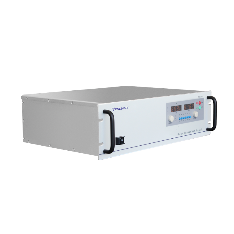
Increasing both wafer throughput and energy efficiency in chemical mechanical polishing appears contradictory at first glance, yet recent high-voltage power system designs have achieved simultaneous gains through intelligent load management, faster transient response, and waste energy recovery that directly enable higher productivity without proportional power increase.
The primary capacity bottleneck in legacy CMP tools is wafer exchange time dominated by electrostatic chuck charging and discharging delays. Next-generation supplies reduce 0-1500 V rise time to under 150 milliseconds through resonant zero-voltage switching topologies operating at 200-400 kHz, while active discharge with energy recovery achieves full de-chuck in 80-120 milliseconds. This shortens load-to-unload cycles by 3-5 seconds per wafer, translating to 15-25% higher wafers per hour on existing hardware.
Parallel processing on multi-platen platforms benefits from centralized power architecture where a single high-capacity backplane supplies multiple platens with dynamic load sharing. When one platen is polishing at full downforce while others are in transfer, available power is automatically redirected, eliminating the need to oversize each platen’s supply for worst-case scenarios. This approach routinely supports four-platen tools operating at 20-30% higher aggregate throughput than individually powered equivalents while using less total power.
Variable voltage operation matched to actual retention requirements provides the core efficiency gain. Rather than maintaining maximum voltage throughout the entire polish cycle, supplies continuously adjust based on real-time downforce and retaining ring pressure data. During low-downforce finishing steps that constitute 30-40% of total polish time, voltage can be reduced by 40-60% with no loss of wafer stability, yielding proportional power savings that compound across hundreds of wafers daily.
Energy recovery during every de-chuck cycle captures 90-95% of stored capacitive energy for reuse, eliminating the several watts of continuous bleed resistor loss present in older designs. In high-throughput tools processing 400+ wafers per day, this alone reduces annual electricity consumption by thousands of kilowatt-hours per tool.
Sleep mode implementation drops quiescent power to under 5 W per platen during extended idle periods while maintaining full high-voltage readiness within 50 milliseconds of wafer present signal. Combined with predictive wake-up triggered by the tool’s scheduler, this virtually eliminates standby losses in real-world fab loading patterns that rarely achieve 100% utilization.
Fast transient response enables aggressive downforce ramping profiles that shorten overall polish time without inducing defects. By supporting 20-30% higher peak removal rates during bulk removal phases while still achieving target planarity through precise finishing control. The power supply’s ability to track these rapid load changes without voltage droop or overshoot is essential for maintaining chucking stability during the resulting acceleration forces.
Multi-zone power systems contribute to both objectives by allowing selective zone deactivation during profile tuning steps. When only center-fast or edge-fast removal is required, up to 70% of zones can operate at minimum voltage or be completely powered down, reducing instantaneous power draw while actually improving removal rate uniformity and therefore reducing overpolish time.
Implementation of these capacity and efficiency improvements has consistently delivered tools capable of 20-35% higher daily wafer starts while reducing average power consumption per wafer by 40-55% compared to previous generation designs, proving that throughput and sustainability targets can be achieved simultaneously through intelligent power system architecture rather than requiring trade-offs.
