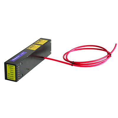
Atomic Layer Etch Self-Limited Reaction Power Supply
Atomic Layer Etching (ALE) represents the ultimate frontier in anisotropic material removal, offering monolayer-by-monolayer precision complementary to Atomic Layer Deposition (ALD). The thermal or plasma-enhanced ALE process typically follows a two-step, self-limiting cycle: Step A) Modification of the surface layer through adsorption or reaction with a precursor gas (e.g., forming a fluorinated layer on silicon); Step B) Selective removal of the modified layer, often via exposure to energetic ions or radicals from a plasma. The "self-limiting" nature—where the modification or removal reaction naturally terminates after one atomic layer—is what grants ALE its unparalleled precision. The power supply energizing the plasma in the removal step (Step B) is not merely an ion source; it is the critical actuator that must deliver energy with a precision matching the atomic-scale process itself, ensuring the removal step is both effective and truly self-limiting.
The primary challenge lies in decoupling ion energy from ion flux, a coupling that is intrinsic to conventional plasma etching. In a standard radio-frequency (RF) plasma, the ion energy incident on the substrate is tied to the plasma potential and the DC self-bias, which are functions of applied power, pressure, and geometry. This makes achieving a self-limited removal step nearly impossible, as increasing ion flux to accelerate the reaction also increases ion energy, leading to unwanted subsurface damage and loss of selectivity. Therefore, ALE power supplies are designed to create a plasma environment where the ion energy can be controlled independently and precisely, often within a window of just a few electronvolts. This is frequently achieved using pulsed or very-high-frequency (VHF) plasmas with separate, dedicated substrate bias supplies.
A common configuration involves an inductively coupled plasma (ICP) source powered by a continuous or pulsed RF generator to create a high-density, low-energy plasma of inert gas (e.g., Ar) and/or reactive radicals. The ions from this plasma are then independently accelerated toward the substrate by a separate, capacitively coupled substrate electrode driven by a specialized bias power supply. This bias supply is the heart of the self-limited removal control. It must deliver short, precise voltage pulses. During the pulse "on" time, a negative voltage is applied, attracting positive ions and imparting to them a kinetic energy defined almost exclusively by the sheath potential, which is controlled by the pulse amplitude. The pulse duration is set to be just long enough for ions to traverse the sheath and strike the surface, but short enough that the total ion dose per cycle is insufficient to sputter unmodified material. The modified surface layer, being chemically altered, has a much lower binding energy and is removed with a low threshold ion energy. Once this monolayer is removed, the underlying pristine material is resistant to further etching at that same ion energy. Thus, the etch stops—it is self-limited.
The design requirements for this bias power supply are extreme. It must generate high-voltage pulses (tens to hundreds of volts) with very fast rise and fall times (to define a sharp ion energy distribution) and a highly stable, flat pulse top (to ensure uniform ion energy). Any droop or noise on the pulse top translates into a spread of ion energies, which can cause incomplete removal of the modified layer or, conversely, begin to attack the underlying material. The repetition rate and duty cycle of these pulses must be synchronized perfectly with the precursor dosing valves of the ALE sequence. Furthermore, the supply must operate into a highly non-linear and dynamic load. The impedance of the substrate electrode changes as the wafer surface chemistry alternates between the modified and pristine states, and the supply's feedback control must compensate for this to maintain pulse shape integrity.
For plasma-enhanced ALE where the modifying chemistry itself is activated by plasma, the main source power supply also requires precise control. It may operate in a pulsed mode, synchronized with the precursor injection, to create a burst of radicals that adsorb and react with the surface until all available sites are occupied, after which the reaction stops. The power level and pulse duration here control the radical density and must be tuned to ensure complete surface saturation without gas-phase nucleation. In all cases, the timing and sequencing of multiple power supplies—source, bias, and possibly remote plasma generators—are orchestrated by a master process controller with millisecond precision. The ALE power supply, therefore, is an instrument of energy dosage control. It delivers not just power, but quantized "packets" of kinetic energy per cycle, tuned to a specific chemical bond strength. This enables the digital subtraction of material one atomic layer at a time, a capability critical for fabricating the ultra-scaled and three-dimensional nanostructures in advanced logic and memory devices.