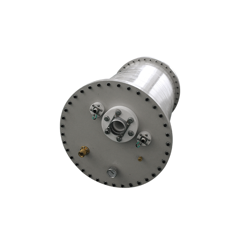
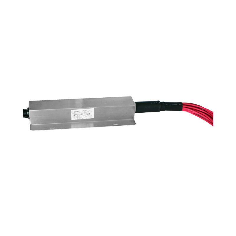
Electron Beam Additive Manufacturing Defect Monitoring Power Supply
Electron Beam Additive Manufacturing (EBAM) is a potent technique for fabricating high-density, complex metal parts in a vacuum environment. Its process integrity hinges on the precise management of the electron beam's energy distribution to create a stable, deeply penetrated melt pool. Defects such as porosity, lack-of-fusion, or keyhole instability can originate from subtle, transient disturbances in beam power, focus, or scanning pattern. Real-time defect monitoring and intervention, therefore, require not only sophisticated sensors but also a high-voltage electron beam power supply capable of executing corrective commands with exceptional speed, precision, and diagnostic fidelity. This supply evolves from a simple beam energizer to the central actuator in a closed-loop defect mitigation system.
The core of the monitoring strategy involves co-axial process observation. High-speed infrared (IR) pyrometers and visual spectrum cameras view the melt pool through the same final aperture as the electron beam. They track metrics like melt pool size, temperature distribution, and plume emission (from vaporization). Advanced systems may also incorporate backscattered electron detectors or plasma charge sensors. When the monitoring algorithms detect an anomaly indicative of an incipient defect—for example, a rapid, localized temperature spike suggesting a keyhole instability, or a drop in plume intensity hinting at gas pore formation—they must generate a corrective signal for the beam. This correction is executed by modulating the outputs of the high-voltage power supply and its associated deflection amplifiers.
The beam power supply itself is responsible for the accelerating voltage (e.g., 60 kV) and the beam current. For defect correction, two primary levers exist: modulating beam current and, to a lesser extent, voltage. A sudden increase in localized heat input, detected as an overheating anomaly, may require an instantaneous reduction in beam current. This places a severe demand on the beam current regulator. It must be capable of a large-signal, fast step-down response without ringing or overshoot. A switch-mode topology with a high-bandwidth current feedback loop is essential. The current setpoint, typically controlled by an analog input, must be updated by the defect monitoring system's digital signal processor (DSP) with microsecond latency. The supply must also provide a high-fidelity, isolated readback of the actual beam current with high bandwidth, as this signal is crucial for correlating power input with sensor output in the diagnostic model.
More nuanced corrections involve high-speed beam deflection, governed by the deflection amplifier power supplies. To break a keyhole instability, the monitoring system might command a rapid, small circular oscillation of the beam or a momentary deflection away from the hotspot. The deflection amplifiers must have a slew rate and bandwidth capable of executing these high-frequency, small-amplitude corrections superimposed on the primary scanning path for the layer. This requires low-inductance, linear or hybrid amplifier designs with stable, low-noise high-voltage rails (typically ±1 kV to ±10 kV). Any noise on these deflection supplies translates directly into beam jitter, which can itself become a source of process variation.
The power supply system must also facilitate, not hinder, the monitoring process. The most significant obstacle is electromagnetic interference (EMI). The switching of the main high-voltage supply and the rapid slew rates of the deflection amplifiers create a tremendous amount of broadband noise. This noise can easily swamp the microvolt-level signals from IR detectors or induce spikes in sensitive photodiode circuits. Therefore, the physical and electrical design of the power supplies must prioritize EMI containment. This involves comprehensive shielding, the use of isolated, filtered DC/DC converters for any internal logic, and careful attention to ground loop management. The synchronization of monitoring sensor exposure times with beam blanking periods can also be orchestrated by the power supply's timing controller to avoid saturating the sensors with direct glow from the molten metal.
Finally, the power supply system serves as a rich source of diagnostic data for post-build analysis and machine learning. Waveforms of beam voltage, beam current, and deflection coil currents are logged synchronously with the camera and pyrometer data. Correlating a subtle dip in beam current (perhaps from space charge effects in an irregular powder layer) with the subsequent formation of a pore provides invaluable data for refining defect prediction algorithms. In this capacity, the power supplies are not just actuators but also high-fidelity sensors of the beam's interaction with the material. Their stability, bandwidth, and noise performance directly define the system's ability to perceive and correct a defect in the few milliseconds available before the moving beam solidifies a flawed track into the part.