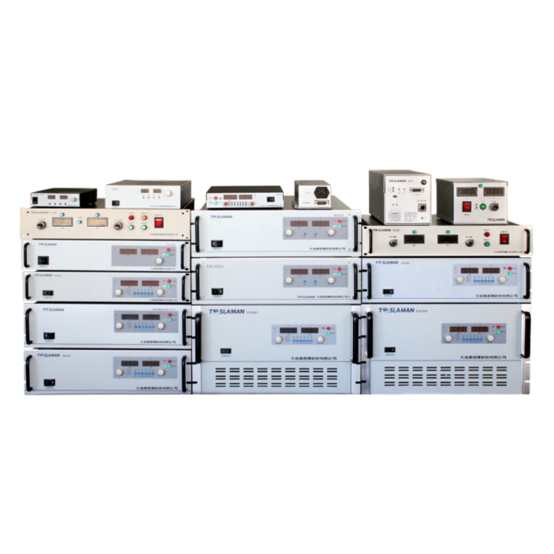
Ion Implantation Transient Enhanced Diffusion Suppression Power Supply
The relentless scaling of semiconductor devices demands ever-shallower and more precisely defined doping profiles. A significant obstacle to achieving these profiles is Transient Enhanced Diffusion (TED), a phenomenon where dopant atoms, particularly boron and phosphorus, undergo accelerated diffusion during the initial stages of post-implantation annealing. This enhancement is primarily driven by the excess interstitial silicon atoms generated by the implantation damage itself. While advanced annealing techniques like flash or laser annealing aim to minimize overall thermal budget, the control of the ion implantation process itself—specifically through the manipulation of the beam's energy, current density, and incident angle—offers a direct method to influence the initial damage state and thereby suppress TED. The high-voltage power supply systems that define the beam's fundamental parameters are thus critical tools for TED mitigation strategies.
TED is intrinsically linked to the density and morphology of the implantation-induced defects. A high concentration of point defects and small defect clusters provides a rich source of interstitials that fuel dopant diffusion. Implantation parameters can be tuned to alter this starting condition. One key approach is to reduce the beam current density. High current density increases the local temperature rise during implantation ("beam heating"), which can cause dynamic annealing in situ. While this might seem beneficial, it often leads to the formation of more stable, extended defects that are potent sources of interstitials during subsequent furnace annealing. A lower current density produces a more amorphous layer with a finer distribution of point-like defects, which may recombine more efficiently during a well-controlled rapid thermal process. The beam current is regulated by the ion source's arc or discharge supply and the extraction power supply. For TED suppression, these supplies must provide exceptionally stable, low-noise current output at precisely controlled, often reduced, levels. Stability is crucial because fluctuations in beam current cause variations in local damage from one region of the wafer to another, leading to non-uniform TED and thus doping profile variability.
The implantation energy, controlled by the main high-voltage acceleration supply, is another powerful lever. Lower energy implants place the peak of the damage profile closer to the surface. This can be advantageous as it allows for a shallower as-implanted profile and positions the damage in a region where surface recombination can efficiently annihilate interstitials. However, very low energies may require novel deceleration or "drift" modes of the implanter. In these modes, ions are extracted at high energy for beam transport stability and then decelerated just before the wafer. This places extreme demands on the high-voltage deceleration power supply. It must provide a stable, low-ripple retarding potential, often in the range of tens of kilovolts. Any voltage ripple or instability during deceleration translates directly into energy contamination (ions with incorrect final energy), which creates a tail in the damage profile and can exacerbate TED. This supply must also be designed to handle secondary electrons and ions generated at the deceleration stage without sparking or instability.
Beyond static parameters, advanced TED suppression techniques involve dynamic modulation during the implant. One such technique is "cold implantation," where the wafer is actively cooled to cryogenic temperatures (e.g., -100°C) to suppress dynamic annealing and preserve a more amorphous, point-defect-rich layer. The power supplies for the beam must operate reliably in this environment, and the thermal load from the beam itself must be carefully managed. More electrically sophisticated methods involve beam "interruption" or pulsed implantation. The hypothesis is that by allowing brief periods of zero beam flux between pulses, point defects have time to recombine before agglomerating into larger clusters. This requires the beam gate or the extraction power supply to operate in a precise, pulsed mode with controllable pulse width and frequency. The rise and fall times of the beam current pulse must be sharp to clearly define the on/off periods, and the average current must remain stable over millions of pulses to maintain dose uniformity. This pushes the beam control power supplies into the domain of high-speed, high-voltage pulsers.
Furthermore, the incidence angle of the beam (controlled by electrostatic or magnetic deflection supplies) can be used for TED control. Off-axis implants can reduce channeling, creating a more controlled damage profile. For ultra-shallow junction formation, a combination of low energy, low current density, and a specific angle is used. The deflection power supplies must therefore provide the precise, stable steering fields needed to maintain this angle consistently across the wafer scan, ensuring the damage profile is uniform.
Integration with metrology is key for a feedback-driven approach. The goal is to implant wafers with a damage profile that is optimal for the subsequent anneal. In-line characterization techniques, like spectroscopic ellipsometry, can measure the thickness of the amorphous layer created by the implant. A closed-loop control system could, in theory, use this measurement to adjust beam current or energy setpoints for subsequent wafers to target an ideal amorphous layer thickness for TED suppression. This would require the high-voltage power supplies to be part of a larger adaptive control framework, accepting setpoint adjustments from a supervisory process controller.
In essence, the power supply systems for TED-suppressed ion implantation are instruments of defect engineering. Their role expands from merely delivering a dose of dopant atoms to carefully sculpting the initial crystal damage with precision and stability. Through control of acceleration/deceleration voltage, beam current, pulsing, and angle, these supplies help create a damage state that is more amenable to interstitial recombination during annealing, thereby minimizing the unwanted diffusion that blurs junction profiles. This capability is fundamental for forming the ultra-shallow, abrupt junctions required in modern CMOS transistors.
