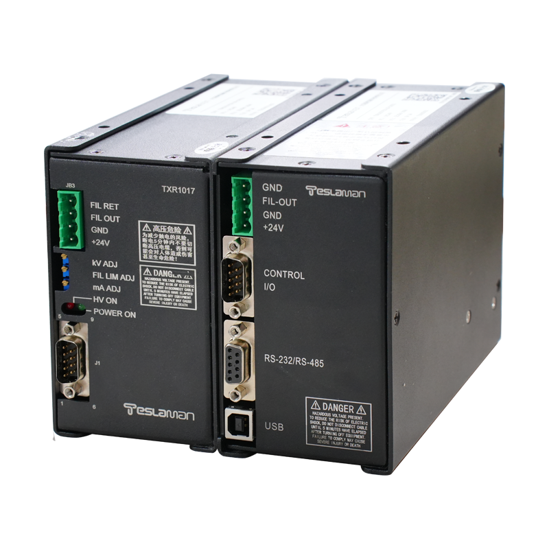
Electrostatic Chuck Wafer Backside Gas Collaborative High Voltage Power Supply
In advanced plasma processing chambers for semiconductor etching and deposition, the electrostatic chuck (ESC) performs the dual, interdependent functions of wafer clamping and precise temperature control. Effective temperature control is predominantly achieved through backside gas (typically helium) delivered to the microscopic gap between the wafer and the chuck surface. The thermal conductance of this gas gap is highly sensitive to the clamping force, which is generated by the electrostatic field. Therefore, the high-voltage DC power supply that provides the clamping voltage and the gas delivery system cannot be operated independently; they must be collaboratively controlled to achieve stable and uniform wafer temperature, a critical parameter for process repeatability. This collaboration requires a sophisticated control architecture where the HV power supply acts as a dynamically responsive element within a thermal management loop.
The underlying physics is governed by contact mechanics and gas dynamics. The electrostatic clamping force, proportional to the square of the applied voltage, flattens the wafer against the chuck, reducing the average gas gap thickness. A thinner gap increases the pressure of the confined helium and improves thermal conductivity. Conversely, a lower clamping force allows the wafer to bow slightly, increasing the gap and reducing thermal coupling. For a given backside gas pressure setpoint, the wafer temperature is directly influenced by the clamping voltage. In a traditional setup, the gas pressure and HV are set to fixed, empirically determined values. This is suboptimal because it ignores process-induced variations. During a high-power etch step, the plasma injects significant heat into the wafer. To maintain a constant temperature, the thermal conductance must increase, which can be achieved by either increasing the backside gas pressure or increasing the clamping force (voltage) to squeeze the gas gap thinner.
A collaborative control system actively manages this relationship. The most common strategy uses wafer temperature as the controlled variable, measured by sensors embedded in the chuck (or inferred from wafer surface sensors). A temperature controller (e.g., a PID loop) calculates an error signal. Instead of adjusting only a heater/chiller or only the gas pressure, this error signal can also drive an adjustment to the ESC high-voltage setpoint. For instance, if the wafer temperature rises above setpoint, the controller could command a slight increase in clamping voltage. This increases the force, compresses the gas gap, improves heat transfer to the chilled chuck, and pulls the temperature back down. This method can be faster than adjusting gas pressure alone, as changing gas pressure involves the time constant of gas flow and plenum filling, whereas the electrostatic force responds almost instantaneously.
This places specific demands on the high-voltage power supply. It must no longer be a simple static DC source but a programmable, dynamically responsive actuator. It needs a control interface (analog input or high-speed digital link) to accept a real-time voltage setpoint from the temperature controller. Its output must be able to follow these changing setpoints smoothly and without overshoot; a step change in clamping voltage could cause a mechanical "jerk" or change local contact points unpredictably. The supply's output stability at any given setpoint remains critical, as ripple on the clamping voltage would modulate the clamping force minutely, potentially causing sub-micron vibrations or thermal flicker.
Furthermore, the collaboration must account for the non-linear and potentially coupled relationship. Changing the clamping voltage affects the electrical impedance between the wafer and chuck, which can influence RF coupling in processes where the ESC is the RF cathode. The control algorithm must be tuned to avoid creating instability in the plasma or interfering with the RF matching network. Additionally, the safe operating window must be respected: excessive voltage could cause arcing, especially if the increased force expels too much helium, creating a local void. Therefore, the control system often includes limiters and rate-of-change limiters on the voltage command.
Advanced multi-zone ESCs add another layer of complexity. For improved temperature uniformity, the chuck may have independently controllable gas pressure zones and corresponding segmented clamping electrodes, each with its own HV supply channel. A collaborative thermal control system can now perform spatial temperature control. If a thermocouple in the chuck's edge zone reports a higher temperature, the system can simultaneously increase the backside gas pressure to the edge zone *and* slightly increase the clamping voltage for the edge electrode segment. This coordinated, multi-input, multi-output (MIMO) control provides a powerful lever for defeating center-to-edge temperature gradients caused by plasma non-uniformity or edge effects. The multiple HV channels must be individually addressable and exhibit matched performance to ensure symmetric response.
Integration and sequencing are also vital. During wafer load, the clamping sequence typically involves first applying a low "pre-charge" voltage to gently pull the wafer flat, then initiating backside gas flow to establish a thermal interface, and finally ramping to the full operational voltage. All these steps are managed by a sequencer that coordinates the HV power supply, the gas valves, and the pressure transducers. Fault recovery procedures must also be collaborative; a loss of backside gas pressure must trigger an immediate reduction in clamping voltage to prevent wafer damage from overheating due to lost thermal contact.
In summary, the collaborative high-voltage power supply for an ESC system is an integral component of a mechatronic thermal control system. Its function transcends simple electrostatic force generation to become a fast, fine-adjustment knob for thermal conductance. Through tight integration with gas pressure control and temperature feedback, it enables the precise and stable wafer temperature regulation required for etching critical dimensions in advanced semiconductor nodes and depositing films with uniform properties across 300mm wafers and beyond.