High-Voltage Regulation for Chemical Amplification in Electron Beam Resist
In electron beam lithography for semiconductor manufacturing, chemically amplified resists (CARs) are the workhorse materials for patterning sub-20nm features. Their operation involves a two-step process: first, exposure by the electron beam generates a latent image of acid catalysts; second, a post-exposure bake (PEB) step thermally drives an acid-catalyzed reaction that amplifies the chemical change, making the resist soluble or insoluble in developer. Recent research explores a third, intervening factor: the application of a controlled electric field during or immediately after exposure, but before PEB, to influence the acid diffusion and reaction kinetics—a process requiring precise high-voltage regulation.
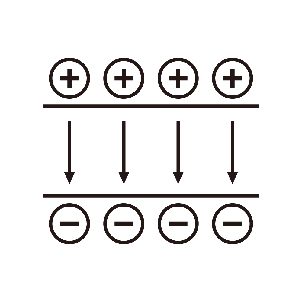
The principle hinges on the fact that the photoacid generator (PAG) molecules in the resist produce mobile hydrogen ions (H+) upon exposure. These protons are the catalyst for the deprotection or cross-linking reaction during PEB. By applying an external electric field across the resist film during the critical period between exposure and PEB, these charged acid molecules can be made to drift. This controlled drift offers several potential levers for process control. Firstly, it can be used to counteract stochastic effects. In extremely small features, the random distribution of a few acid molecules can lead to line edge roughness. An applied field could provide a slight directional bias, smoothing out these statistical fluctuations. Secondly, it could enhance or suppress chemical amplification in specific areas. For dense patterns where acid diffusion from neighboring exposed areas causes unwanted reactions (proximity effect), a carefully shaped field could confine acid migration.
Implementing this requires a high-voltage system integrated into the lithography tool's wafer stage. The stage must be modified to include a planar electrode beneath the wafer and a top electrode, often a transparent conductive layer, above the resist-coated wafer with a small gap. The high-voltage supply applies a potential difference, creating an electric field perpendicular to the wafer plane. The field strength is moderate, typically on the order of 0.1 to 1 MV/m, meaning a few volts across a 100nm resist film, but this requires a stable supply capable of outputting up to several hundred volts with millivolt precision due to the tiny gaps involved.
The timing and waveform of the applied voltage are critical parameters. The field may be applied as a constant DC bias during the entire exposure and delay period, or as a pulsed field synchronized with the beam blanking. More complex schemes involve field gradients or switching polarity. The power supply must therefore be highly programmable, capable of generating complex low-noise waveforms. Furthermore, it must be compatible with the vacuum environment of the e-beam tool and must not interfere with the primary beam deflection or detection systems. This necessitates extensive shielding and grounding studies to ensure the high-voltage field does not deflect the low-energy secondary electrons used for alignment or inspection.
Characterization and modeling are immense challenges. The effect of the field on acid diffusion coefficients, reaction rates, and ultimate linewidth is a complex function of resist chemistry, bake conditions, and pattern geometry. Developing a usable process requires building a new physical model that incorporates electro-diffusion equations. The high-voltage supply system becomes part of the process calibration kit, with its output parameters (magnitude, timing, profile) being tuned alongside exposure dose and PEB temperature. This adds a layer of complexity but also a powerful new degree of freedom for overcoming fundamental resolution limits.
Practical integration also considers wafer charging. The electron beam itself charges the resist surface. The external field application must account for this pre-existing charge distribution to avoid unpredictable results. This may require in-situ charge monitoring and dynamic adjustment of the applied voltage. While still primarily a research topic, the integration of high-voltage field control into the e-beam lithography process flow represents a frontier in directed self-assembly at the molecular scale, where the power supply acts as a director for chemical reactions, pushing beyond the boundaries of traditional optical and thermal process knobs.
