High-Voltage Control for Sidewall Morphology in Reactive Ion Deep Etching
Reactive Ion Etching (RIE), and particularly its deep variant (Deep RIE or the Bosch process), is the workhorse technology for creating high-aspect-ratio microstructures in silicon for MEMS, advanced packaging, and through-silicon vias. A key challenge in these processes is the control of sidewall morphology—specifically, achieving vertical, smooth sidewalls while managing the characteristic scalloping profile inherent to time-multiplexed etching and passivation cycles. The high-frequency RF power supply used to generate the plasma is a primary lever for this control, but the independent DC bias voltage that develops on the wafer chuck, or is actively controlled via a separate low-frequency or DC power supply, is the dominant factor influencing ion bombardment energy and, consequently, sidewall anisotropy and smoothness.
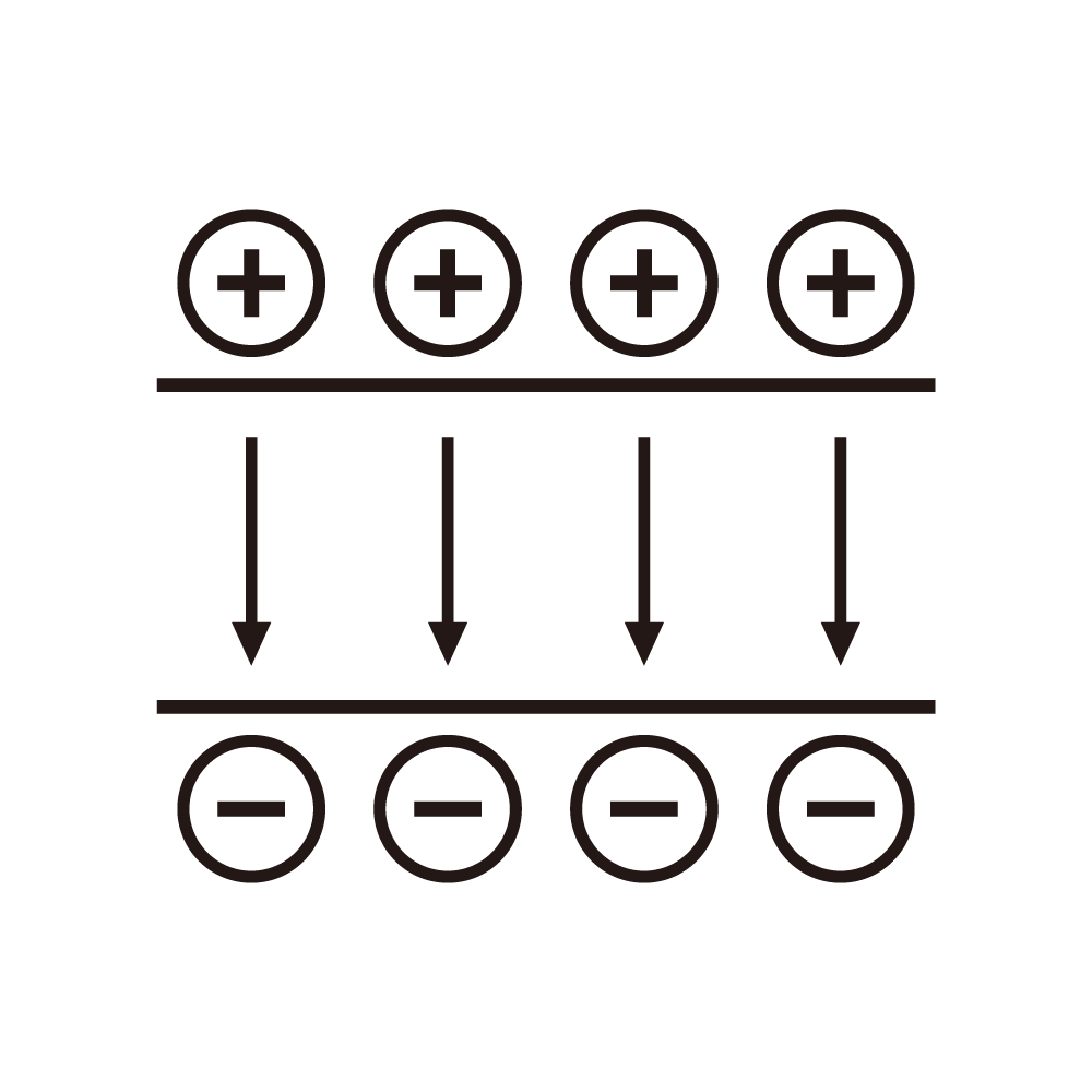
In a typical parallel-plate RIE reactor, the wafer sits on a powered or grounded electrode. The RF power, at 13.56 MHz or similar, creates the plasma. Due to the mobility difference between electrons and ions, a negative DC self-bias voltage (Vdc) naturally develops on the RF-powered electrode. This voltage accelerates positive ions from the plasma vertically downward onto the wafer. In the Bosch process, which alternates between an etching cycle (using SF6 plasma) and a passivation cycle (using C4F8 plasma), the ion energy during the etch cycle is critical. It determines the directionality of the etch. High-energy ions bombard primarily the horizontal surfaces, etching the bottom of the trench, while the sidewalls are protected by the Teflon-like polymer deposited during the passivation cycle.
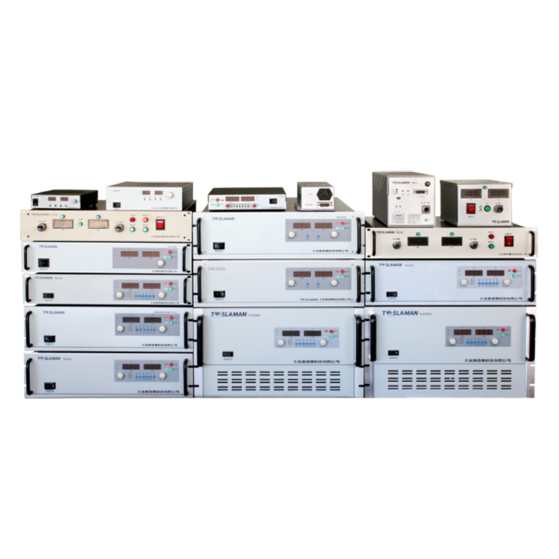
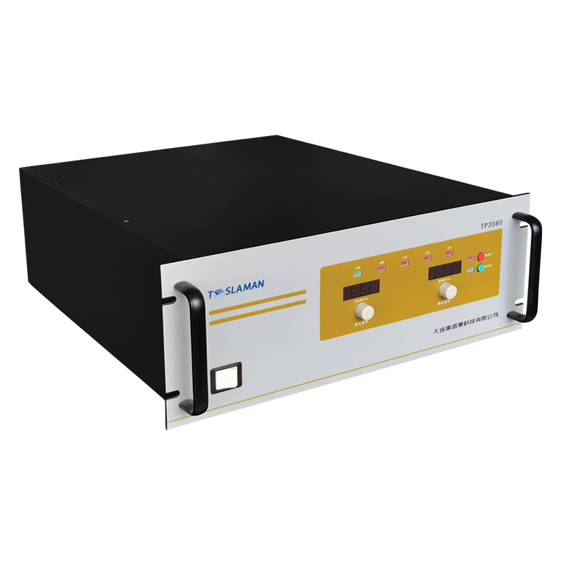
Active control of this bias voltage, separate from the main RF plasma power, provides a powerful knob for sidewall tuning. This is achieved by superimposing a low-frequency (100s kHz) or DC bias onto the wafer chuck via a dedicated high-voltage power supply, often integrated with the main RF matching network. By independently adjusting this bias voltage, the energy of ions striking the wafer can be decoupled from the plasma density (which is primarily controlled by the main RF power).
To achieve smooth sidewalls, the goal is to minimize the lateral etching component during the brief periods when the sidewall passivation is imperfect or temporarily removed. A higher bias voltage increases ion energy, which has two competing effects. It increases the vertical etch rate, which is desirable. However, if the energy is too high, ions can cause sputtering or ion-enhanced chemical etching of the sidewall polymer, leading to lateral etching, bowing, or increased surface roughness (scalloping). Conversely, a bias that is too low results in insufficient ion energy to efficiently break chemical bonds at the trench bottom, causing reduced etch rate and allowing more time for isotropic chemical etching to undercut the mask.
Advanced process control uses real-time monitoring, such as optical emission spectroscopy or RF harmonic analysis, to infer plasma conditions. The bias power supply is then dynamically adjusted within each etch cycle. For instance, at the beginning of an etch cycle, a slightly higher bias may be used to quickly clear any residual passivation from the trench bottom. The bias can then be reduced to an optimal value for the bulk of the etch step to maintain anisotropy. Just before switching to the passivation cycle, the bias might be briefly modulated to help shape the trench bottom or clean the sidewall bases.
Furthermore, for etching novel materials or achieving ultra-smooth sidewalls, techniques like pulsed biasing are employed. Here, the DC bias is applied in short, high-energy pulses synchronized with the main RF. This allows high instantaneous ion energy for directional etching, while the time-averaged energy is kept lower, reducing sidewall damage and heating. The design of such a pulsed bias supply requires careful attention to rise time, pulse shape, and synchronization jitter to ensure process repeatability.
This precise, independent control of ion bombardment energy through a dedicated high-voltage bias system is essential for pushing the limits of deep silicon etching. It enables the fabrication of MEMS structures with optically smooth sidewalls for inertial sensors, high-aspect-ratio interconnects with uniform electrical properties, and microfluidic channels with defined surface characteristics. It transforms the etch process from a broadly tunable recipe into a finely sculpting tool, capable of producing three-dimensional microstructures with nanoscale precision in the vertical profile.
