Multi-Step Response Optimization for Electrostatic Chuck High-Voltage Systems
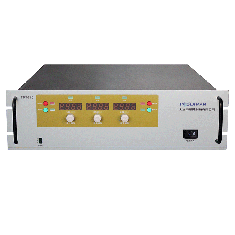
Electrostatic chucks have become indispensable components in semiconductor processing equipment, providing a non-mechanical means of clamping wafers during lithography, etching, and deposition steps. Their operation relies on applying a high voltage to embedded electrodes within the chuck, inducing opposite charges on the wafer backside and creating a clamping force through Coulombic attraction. The increasing complexity of process sequences, particularly those involving rapid thermal cycling, plasma modulation, or sequential processing steps with different clamping requirements, has placed new demands on the high-voltage power supply system. Simple on/off clamping is no longer sufficient; advanced processes require a high-voltage system capable of executing complex, multi-step voltage profiles with precise timing, minimal overshoot, and stable holding states—a discipline we can term multi-step response optimization.
The fundamental challenge lies in the nature of the electrostatic chuck as a load. It presents a highly capacitive and often non-linear impedance to the power supply. When a voltage step is commanded—for instance, to transition from a low clamping force for alignment to a high force for processing—the supply must charge this large capacitance quickly. However, a brute-force fast charge can lead to significant overshoot and ringing due to parasitic inductance in the cables and the chuck's internal structure. Overshoot is not merely an electrical anomaly; it can cause instantaneous over-clamping, inducing stress in the wafer or even attracting particulate contamination. Conversely, an excessively slow charge can extend process cycle time and may allow the wafer to shift during the transition phase.
An optimized multi-step response system addresses this through several layers of control. First, the high-voltage power supply itself must have a fast, stable control loop. Modern designs utilize digital signal processors to implement sophisticated charging algorithms. Instead of a simple step command, the controller can execute a shaped voltage ramp. This profile might have an initial high-current phase to charge the bulk capacitance quickly, followed by a carefully tapered approach to the final setpoint to eliminate overshoot. The parameters of this ramp (slew rate, taper point) can be programmed based on the known capacitance of the chuck and wafer type, which can vary significantly between thin, warped wafers and standard substrates.
Second, the system must manage transitions between distinct voltage levels that represent different operational modes. A common sequence might involve: Step 1) applying a low voltage for initial wafer attraction and alignment; Step 2) ramping to an intermediate voltage for plasma ignition and stabilization; Step 3) stepping to the full process voltage for main etch or deposition; and finally Step 4) executing a controlled discharge sequence for wafer release. Each transition must be executed with the same care as the initial charge. The discharge sequence is particularly critical; a rapid discharge can cause the wafer to pop off the chuck with enough force to generate particles or damage backside films. An optimized system often employs an active discharge circuit that pulls the voltage down in a controlled manner, sometimes even through a negative voltage phase to neutralize residual charge.
Furthermore, the system must account for real-time disturbances. During plasma processing, the potential of the wafer surface can float, effectively modulating the clamping field. Some advanced electrostatic chucks incorporate a bipolar design or a separate RF bias electrode. The high-voltage DC clamping supply must be isolated from and immune to the MHz or kHz noise from the plasma power supplies and RF bias generators. This requires exceptional common-mode rejection in the supply's feedback circuitry and often the use of optical isolation for control signals. Additionally, the supply may need to adjust its output dynamically in response to a measured parameter, such as chucking force inferred from a pressure sensor, forming a closed-loop clamping force control system.
Integration with the equipment's safety and recipe management system is paramount. Each step in the voltage profile is tied to specific stages of the process recipe. The high-voltage controller must receive precise triggers from the main equipment controller and confirm successful completion of each step before allowing the process to proceed. Diagnostic capabilities are built-in, monitoring for arc events (which can damage the chuck's dielectric layer), leakage current (indicative of contamination or dielectric breakdown), and temperature-dependent performance drift.
In practice, this level of optimization transforms the electrostatic chuck from a simple clamp into an active, programmable process component. It enables new capabilities such as zone-specific clamping to counteract wafer bow during rapid thermal processing, or dynamic force reduction during certain plasma steps to minimize pattern shifting. The high-voltage system, through its precise and predictable multi-step response, ensures wafer stability, minimizes particulate generation, and enhances process yield—critical factors in the production of advanced semiconductor devices where nanometer-scale precision is required.