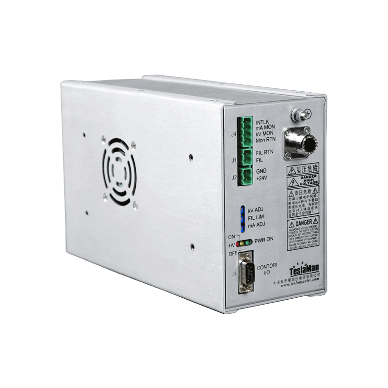
High-Voltage Optimization of Wafer Contact Thermal Resistance in Electrostatic Chucks
Thermal management within a plasma processing or vacuum deposition chamber is as critical to process yield as the plasma chemistry itself. The electrostatic chuck serves as the primary thermal pathway between the wafer and the temperature-controlled pedestal. While the chuck provides the necessary clamping force, its role as a thermal interface is equally vital. The high voltage applied to the chuck not only generates the clamping force but also directly and significantly influences the thermal contact resistance at the wafer-chuck interface. Optimizing the applied voltage waveform and magnitude to minimize thermal resistance while ensuring uniform clamping and rapid de-clamping is a sophisticated high-voltage engineering challenge.
The thermal contact between the backside of the silicon wafer and the top surface of the electrostatic chuck is never perfect. Micron-scale roughness and inherent wafer curvature create microscopic air gaps. To improve heat transfer, a backside gas, typically helium, is introduced at a controlled pressure. The effectiveness of this gas conduction is highly dependent on the gap distance. The clamping force generated by the high-voltage potential directly compresses the wafer against the chuck surface, flattening the wafer and reducing the gap height. A higher clamping force results in a smaller gap and lower thermal resistance. However, this relationship is not linear and reaches a point of diminishing returns. Furthermore, excessive force can induce stress in the wafer, causing slip dislocations in epitaxial layers or even fracturing fragile wafers.
An optimized high-voltage system for thermal management does not simply apply a fixed voltage. It recognizes that the required clamping force, and hence the optimal voltage, is a function of the helium backside pressure and the process power being applied to the wafer. In a high-density plasma etch process, the wafer receives a substantial heat flux. During this step, the high-voltage supply may be commanded to its maximum safe output to minimize thermal resistance and keep the wafer cool. During a subsequent idle or metrology step, the voltage can be reduced to minimize stress and power consumption. This requires the high-voltage supply to be capable of executing a programmed profile, stepping or ramping the output voltage in coordination with the process recipe. The transition must be managed carefully; a sudden reduction in voltage could cause a momentary reduction in clamping force, allowing the helium pressure to physically lift the wafer, a catastrophic event.
Another dimension of optimization involves the spatial uniformity of the clamping force. Large wafers are not perfectly flat; they exhibit global bow and local topography. A single, uniform voltage applied to a single, contiguous electrode will not produce a uniform clamping force. Advanced electrostatic chucks feature multiple, independently controllable electrodes arranged in concentric zones. Each zone can be biased with a different high voltage. This allows for a tailored pressure profile that compensates for wafer curvature, ensuring that the helium gap is uniform from center to edge. Thermal uniformity is thus directly dependent on the performance of the multi-channel high-voltage system. Each channel must be independently programmable and exhibit the same low-drift, low-ripple characteristics as the single-channel system, while also being immune to cross-talk from adjacent zones. This is a non-trivial power supply design task, requiring careful isolation and often the use of separate transformer windings for each channel.
The interaction with helium pressure is a closed-loop control problem. The heat transfer coefficient is proportional to the gas pressure, but the pressure itself is limited by the clamping force. If the helium pressure is too high relative to the clamping force, the wafer will lift. To maximize cooling, one operates at the highest possible helium pressure that still maintains intimate contact. This is an ideal application for an active control system. A sensor, often a capacitive gauge measuring the exact gap distance, provides a feedback signal. The high-voltage controller then adjusts the clamping voltage up or down to maintain a target gap distance, allowing the helium pressure to be set to a high, fixed value. This is known as constant-gap control and is the gold standard for thermal management in critical etch processes. The high-voltage supply, in this role, is not a static power source but a servo actuator in a precision mechanical positioning loop.
Diagnostics and reliability are also key. The integrity of the dielectric layer on the chuck is paramount. A pinhole defect can lead to a short circuit from the electrode to the wafer, causing immediate voltage collapse and potential damage. Advanced high-voltage systems include sensitive leakage current monitoring. By analyzing the minute current that flows through the dielectric during normal operation, the system can detect early signs of degradation, such as increasing conduction or micro-arcing. This predictive diagnostic capability allows for proactive maintenance, preventing unscheduled downtime and yield loss.
Finally, the de-clamping phase requires its own specialized voltage optimization. When the process is complete, the wafer must be released. Simply turning off the high voltage is insufficient due to residual charge trapped in the dielectric layer or on the wafer backside. This residual charge creates a persistent electrostatic force, causing the wafer to stick. An optimized supply includes a controlled de-clamping sequence, often involving the application of a reverse polarity voltage of carefully calculated magnitude and duration to neutralize the trapped charge. This sequence must be fast enough for high throughput yet gentle enough to avoid creating a plasma discharge that could damage the wafer or the chuck.
In conclusion, the high-voltage supply for an electrostatic chuck has evolved far beyond a simple clamp power source. It is a multi-functional, adaptive instrument for active thermal management. By optimizing voltage magnitude, spatial distribution, dynamic sequencing, and integrating with gas pressure control and residual charge neutralization, it ensures that the delicate thermal balance required for advanced semiconductor processing is maintained with precision and reliability.