High-Voltage Control for High-Aspect-Ratio Features in Reactive Ion Etching
Reactive Ion Etching is a foundational process in semiconductor manufacturing for transferring mask patterns into underlying films with high fidelity. The relentless drive towards smaller device nodes and three-dimensional architectures, such as fin field-effect transistors and vertical NAND memory, has placed immense demands on the etching process. Creating features with extremely high aspect ratios, often exceeding 100:1, while maintaining vertical sidewalls and avoiding defects like bowing, twisting, or aspect-ratio-dependent etching, requires exquisite control over the plasma environment. A critical, and often underappreciated, actuator in this control is the high-voltage bias applied to the substrate. This voltage, which determines the energy and directionality of ions bombarding the wafer, is not a static parameter but must be dynamically controlled throughout the etch process to achieve the desired profile.
In a typical RIE chamber, a plasma is generated using a radiofrequency power source applied to an upper electrode or an inductively coupled coil. This creates a dense plasma with a self-bias potential. However, to independently control ion energy, a separate radiofrequency bias power supply is applied to the wafer chuck, which is also an electrode. This bias supply, operating typically at frequencies from 400 kilohertz to 13.56 megahertz, generates a negative direct current self-bias voltage on the wafer surface. The magnitude of this bias voltage, often ranging from a few tens of volts to several kilovolts, determines the energy with which ions strike the wafer. Higher energy leads to more directional, anisotropic etching, but also increases the risk of damage to the mask and substrate, and can exacerbate microloading effects.
For high-aspect-ratio etching, the challenge is that the optimal ion energy is not constant throughout the etch. At the beginning, when the feature is shallow, a moderate bias is sufficient to clear the bottom of the feature and maintain anisotropy. As the feature deepens, the flux of reactive neutrals to the bottom decreases due to transport limitations, while the flux of ions, being directional, remains relatively high. This can lead to a phenomenon known as notching or aspect-ratio-dependent etching, where the bottom of the feature etches faster than the top. To compensate, the bias voltage may need to be reduced as the etch progresses to balance the ion-to-neutral ratio at the feature bottom. Conversely, if the sidewall passivation is insufficient, a higher bias might be needed to enhance sputtering of redeposited material.
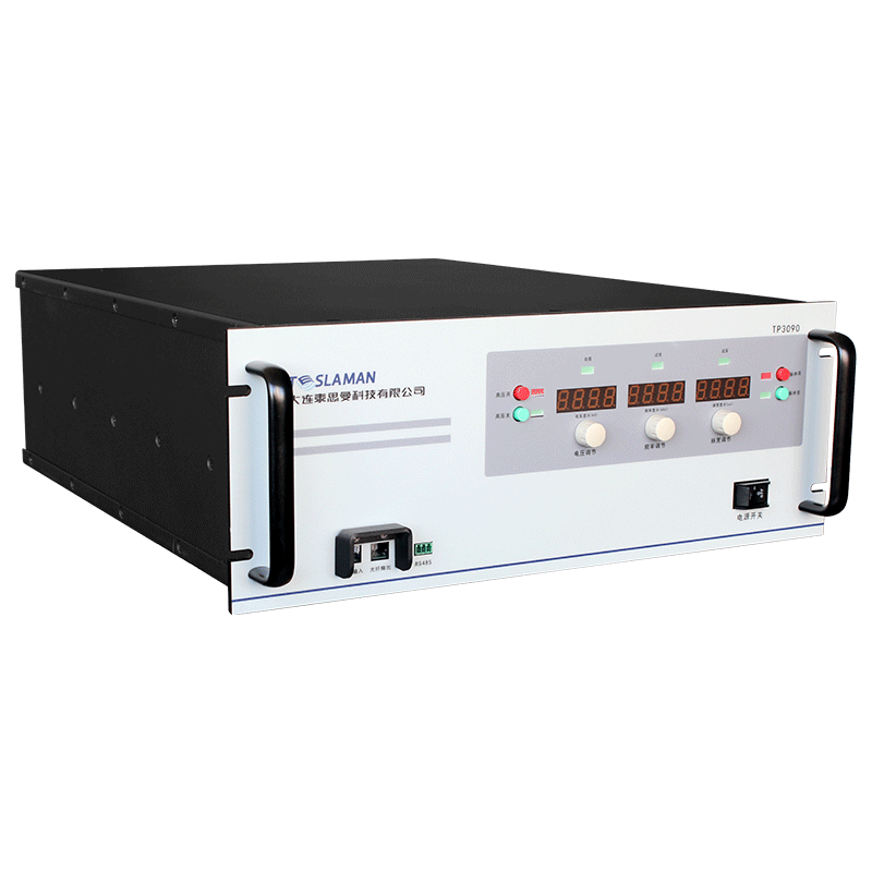
This dynamic control requires the bias power supply to be fully programmable and capable of executing a complex voltage waveform or a multi-step voltage recipe. The supply must be able to change its output voltage smoothly, without overshoot or ringing, as a function of time or in response to an endpoint signal. The transition from one voltage level to another must be fast enough to keep pace with the etch rate, but not so fast as to cause instability in the plasma sheathe. This is typically achieved using a digital control loop that can modulate the radiofrequency amplitude in real-time.
Another advanced technique for high-aspect-ratio etching is the use of pulsed biasing. Instead of a continuous sine wave, the bias power is turned on and off at a low frequency, typically a few kilohertz. During the on-time, ions are accelerated towards the wafer with high energy. During the off-time, the plasma sheathe collapses, allowing electrons to reach the wafer and neutralize any accumulated charge. This charge neutralization is critical for preventing aspect-ratio-dependent charging, where ions can be deflected by local electric fields built up in the feature, causing twisting or bowing. The high-voltage bias supply for pulsed operation must have an extremely fast rise and fall time, and the timing of the pulse must be precisely synchronized with the main plasma source to control the electron and ion dynamics.
Furthermore, the bias supply must be capable of operating with very low harmonic distortion. Harmonics in the bias waveform can create multiple ion energy peaks, leading to a spread in ion energies and a loss of anisotropy. The output stage of the supply is typically a linear or class-D amplifier with sophisticated filtering to ensure a clean, single-frequency output.
Integration with metrology and endpoint detection is also crucial. Optical emission spectroscopy or interferometry can be used to monitor the etch depth or the clearing of a layer. The bias supply's control system can use this signal as a feedback input, adjusting the bias voltage to maintain a constant etch rate or to achieve a specific profile. This closed-loop control transforms the etch process from a timed recipe into an adaptive, self-optimizing operation.
In the production of modern memory and logic chips, the ability to etch deep, narrow trenches and holes with atomic-scale precision is what enables the continued scaling predicted by Moore's Law. The high-voltage bias supply, once a simple accessory, has become a primary tool for plasma engineering. Its dynamic range, waveform purity, and programmability are directly correlated with the ability to create the three-dimensional structures that define the performance of today's and tomorrow's electronic devices.