The Role of High Voltage in Minimizing Detection Limits for Ion Implantation Process Control
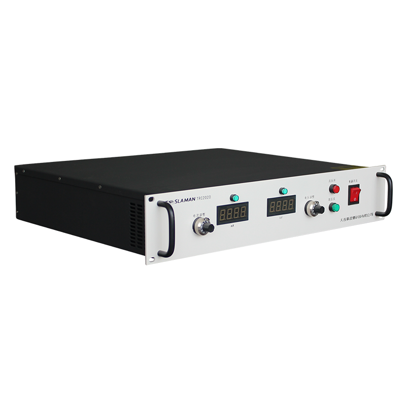
In the realm of modern semiconductor manufacturing, ion implantation stands as a critical process for doping silicon wafers to modify their electrical properties. As device geometries shrink to the nanometer scale and new architectures like gate-all-around transistors emerge, the industry faces a profound challenge: the need for ultra-low energy and ultra-low dose implants. These precise requirements push the boundaries of not only the implanters themselves but also the metrology used to verify the process. For a veteran engineer, the relationship between the high voltage systems and the detection of these minute dose levels becomes a fascinating study in applied physics and instrumentation. The core of the issue lies in the fact that traditional dosimetry, often based on integrating the electrical current delivered by the ion beam directly to the wafer, becomes exceedingly difficult at low beam currents. The signal-to-noise ratio plummets, making it nearly impossible to distinguish the true implant current from background noise and leakage currents within the end station. This is where the ancillary high voltage biasing of detection apparatuses plays a pivotal, yet often underappreciated, role. In many modern implanters, or in dedicated metrology tools used for dose verification like Therma-Wave or other non-contact measurement systems, the sensitivity to ultra-low doses is intrinsically linked to the stability and purity of the voltages applied to the detectors themselves. For instance, in systems that rely on collecting secondary electrons or measuring the surface photo-voltage of the implanted wafer, the accuracy of the measurement hinges on the ability to establish a precise and unwavering electric field. A high voltage power supply, if it exhibits ripple or drift, injects noise directly into the measurement. Imagine trying to measure a photo-voltage change induced by a 1e10 atoms/cm² implant, which represents a minuscule fraction of a monolayer. Any fluctuation in the bias voltage applied to a nearby electrode or the detector itself will swamp this delicate signal. Over the decades, we have seen a relentless push for high voltage modules with ripple specifications in the parts-per-million range and thermal drift coefficients that are effectively negligible. This is not merely about providing a potential; it is about providing a perfectly silent, stable electrostatic environment. Furthermore, the design of the cabling and feedthroughs becomes critical. A seemingly minor discharge or leakage current in a high voltage cable, perhaps caused by contamination in the vacuum interface, can generate spurious currents that are orders of magnitude larger than the signal from the ultra-low dose implant. Therefore, the application of high voltage in this context is as much about material science and system architecture as it is about power electronics. The high voltage must be delivered with a purity that preserves the quantum of information we are trying to extract from the wafer, enabling the process control necessary for the most advanced integrated circuits.