Adaptive High-Voltage Modulation for Ion Implantation Scanning Systems
Ion implantation has long stood as a cornerstone process in the semiconductor industry and in advanced materials modification. In my fifty years of engagement with high-voltage technologies, I have witnessed the evolution of ion implanters from relatively simple machines to extraordinarily complex systems capable of precisely placing atoms within a crystalline lattice. At the heart of this precision lies not only the ion source and the beamline optics, but also a often-overlooked component: the high-voltage modulation system that controls the final beam energy as it scans across the wafer. The concept of adaptive frequency modulation in this context represents a significant leap forward in our ability to achieve uniformity and control dose accuracy at the atomic scale.
The fundamental principle of ion implantation involves generating ions, accelerating them through a high-voltage potential, and then directing them onto a substrate. The depth to which these ions penetrate is determined primarily by their energy, which is a direct function of the acceleration voltage. For many years, this voltage was maintained at a fixed, stable level, and the beam was scanned electrostatically or mechanically across the wafer. However, as device geometries have shrunk into the nanometer regime, the tolerance for dose non-uniformity and energy contamination has become almost vanishingly small. This is where adaptive high-voltage modulation enters the picture, not as a simple constant bias, but as a dynamically varying parameter synchronized with the beam scanning motion.
The challenge originates from the fact that the effective angle of incidence and the path length through any intervening layers or the wafer itself can vary as the beam is scanned. In a typical electrostatic scanning system, the beam is deflected by applying time-varying voltages to a pair of deflection plates. As the beam sweeps from the center to the edge of the wafer, the angle at which it strikes the surface changes. This variation in angle can lead to differences in the effective junction depth and can also cause shadowing effects in the presence of topographical features on the wafer. To compensate for this, one can dynamically adjust the acceleration voltage as a function of the beam position, ensuring that the vertical component of the ion energy, and thus the penetration depth, remains constant across the entire wafer diameter.
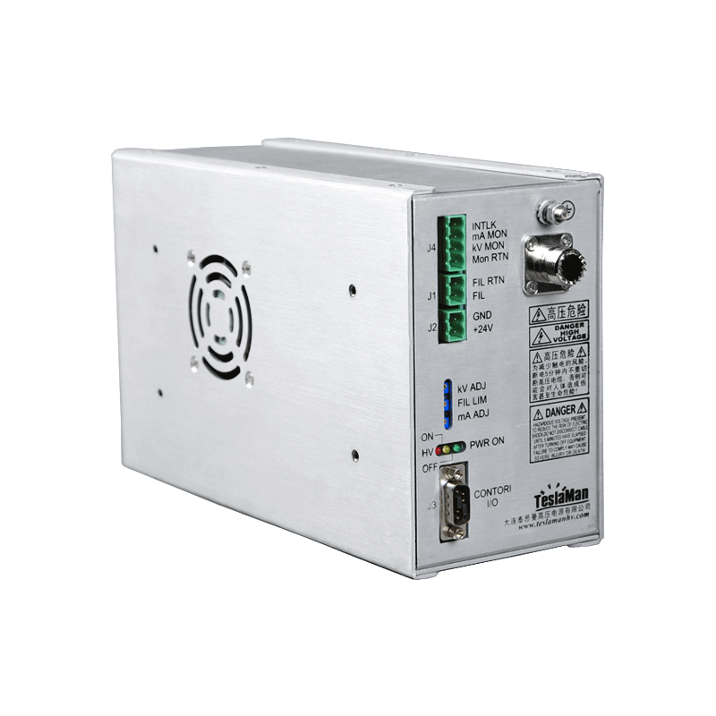
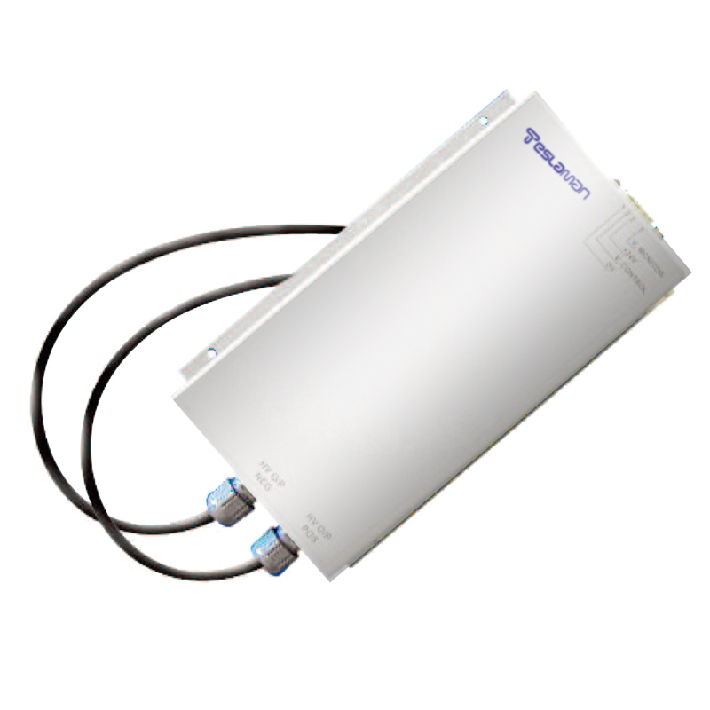
The implementation of such a system demands a high-voltage power supply with an exceptionally fast and precise response. The modulation frequency must be synchronized with the scan frequency, which can range from a few hertz for mechanical scanning to several kilohertz for electrostatic scanning. The power supply must be capable of altering its output voltage by hundreds or even thousands of volts within microseconds, while maintaining absolute stability and purity of the output waveform. Any ringing, overshoot, or droop in the voltage during this modulation will directly translate into an error in the ion energy and, consequently, in the implantation depth.
Furthermore, the concept of adaptivity extends beyond simple position-based compensation. In modern ion implanters, the beam current is not always constant. It can fluctuate due to changes in the ion source plasma, space charge effects, or even the gradual contamination of beamline components. An adaptive high-voltage modulation system can be designed to respond to these fluctuations in real-time. By monitoring the beam current upstream and downstream of the acceleration gap, the control system can calculate the instantaneous space charge within the beam. This space charge effectively alters the potential that the ions experience. An adaptive supply can modulate the applied voltage to counteract this dynamic space charge effect, maintaining a constant net accelerating potential for the ions regardless of beam current variations. This is a form of feed-forward control that requires an intimate understanding of beam physics and a power supply architecture capable of implementing complex, non-linear correction algorithms.
The design of the high-voltage amplifier for this task is a specialized discipline. Traditional linear amplifiers, while offering excellent fidelity, are inefficient and generate enormous heat when called upon to deliver the kind of high-voltage swings required at high frequencies. Switch-mode topologies, particularly those based on resonant or multi-level converters, have become the preferred solution. These designs can achieve high efficiency and fast transient response. The output stage must be carefully shielded to prevent electromagnetic interference from corrupting the beam diagnostics or other sensitive electronics in the implanter. The high-frequency transformer within the modulator must be designed for minimal inter-winding capacitance to ensure that common-mode currents do not create ground loops, which could introduce noise into the beam energy.
In my laboratory, we have explored the limits of this technology by attempting to create ultra-shallow junctions for next-generation transistors. The requirement was to implant ions at energies so low, below 200 electronvolts, that the beam transport becomes extraordinarily difficult due to space charge blow-up. We employed a technique called drift mode, where the ions are extracted at a higher energy and then decelerated just before the wafer by applying a positive bias to the wafer itself. This deceleration potential must be modulated adaptively in sync with the scanner to ensure that the final landing energy is constant. The power supply for this task had to provide a precisely controlled, variable voltage from zero to several kilovolts, with the ability to change that voltage in lockstep with the scanning frequency. The results demonstrated that with the right adaptive high-voltage control, we could achieve junction depths that were previously thought impossible with conventional beamline implanters.
The adaptive modulation also plays a critical role in preventing charge build-up on insulating wafers or on wafers with insulated features. As the beam scans, it deposits charge. If this charge is not neutralized, it can create local electric fields that deflect the incoming beam, distorting the intended dose pattern. This is often managed by a separate electron flood gun, but the bias on the wafer can also be modulated to attract or repel electrons from this flood gun, optimizing the charge neutralization process across the entire wafer surface. This requires the high-voltage bias supply to be capable of producing complex waveforms, perhaps a DC level with a superimposed AC component, all while the main acceleration voltage is being adaptively modulated for depth control. The coordination of these multiple, simultaneous modulation tasks places extreme demands on the power supply control architecture, necessitating the use of high-speed digital signal processors and sophisticated feedback algorithms that are the culmination of decades of research in power electronics and plasma physics.