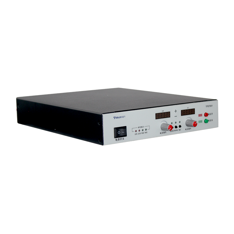
High-Voltage Topologies with Power Factor Correction for Electrostatic Chuck Applications
The electrostatic chuck has become an indispensable component in semiconductor manufacturing equipment, providing the means to clamp and thermally manage silicon wafers during critical etching and deposition processes. These chucks require high-voltage power supplies, typically in the range of several hundred volts to a few kilovolts, to generate the electrostatic force. While the power demanded by a single chuck is not enormous, a modern semiconductor fab contains hundreds of process tools, each with multiple chucks, and the aggregate power consumption is substantial. Furthermore, these tools are often connected to the same facility power grid, and the non-linear loads presented by conventional high-voltage power supplies can cause significant power quality issues, including harmonic distortion and a poor power factor. This has driven the development of advanced high-voltage power supply topologies that incorporate power factor correction. In my five decades of designing power systems for the semiconductor industry, I have seen power factor correction evolve from an afterthought to a primary design requirement, driven by both utility company regulations and the need for overall facility efficiency and reliability.
The term power factor describes how effectively electrical power is converted into useful work. A load with a low power factor draws more current than necessary for a given amount of real power, leading to losses in the distribution system and potentially exceeding the capacity of transformers and wiring. The classic high-voltage power supply for an electrostatic chuck often uses a line-frequency transformer to step up the voltage, followed by a rectifier and a filter capacitor. This topology draws current from the AC line in short, high-amplitude pulses near the peaks of the voltage waveform, resulting in a very low power factor and high harmonic distortion. The solution is to incorporate an active power factor correction stage at the front end of the power supply. This stage, typically a boost converter operating at a high switching frequency, actively shapes the input current waveform to be sinusoidal and in phase with the line voltage, presenting a near-unity power factor load to the AC mains.
The design of a high-voltage supply with power factor correction for an electrostatic chuck presents several unique challenges. First, the output voltage must be highly stable and free of ripple. The electrostatic clamping force is proportional to the square of the voltage, so any ripple in the output will cause a fluctuating force, which can lead to vibration or inconsistent thermal contact. The power factor correction stage, which operates at a high frequency, can generate switching noise that must be carefully filtered to prevent it from appearing on the high-voltage output. This requires a multi-stage filtering approach, with careful attention to grounding and shielding. Second, the electrostatic chuck itself is a highly capacitive load. The power supply must be able to charge this capacitance quickly during the clamping cycle, and it must be able to discharge it safely when the wafer is to be released. This requires a bidirectional capability, or at least a means of dissipating the stored energy. A simple diode rectifier output stage cannot sink current, so a more complex topology, such as a bidirectional flyback or a full-bridge converter, may be required.
Another critical consideration is the dynamic response of the power supply. In a plasma processing environment, the electrostatic chuck may experience sudden changes in the load due to plasma ignition or arcing. The power supply must be able to maintain its output voltage despite these disturbances. The power factor correction stage, which has its own control loop, must not interfere with the high-voltage control loop. The two control systems must be carefully coordinated to ensure stability under all operating conditions. The topology choice also affects the overall efficiency and thermal management. A high-frequency switching topology with power factor correction can achieve efficiencies well above 90%, which is crucial for reducing the heat load in the cleanroom environment. The use of modern wide-bandgap semiconductors, such as silicon carbide, allows for even higher switching frequencies and lower losses, enabling more compact and efficient designs. In my experience, the integration of power factor correction into high-voltage supplies for electrostatic chucks is a perfect example of how seemingly separate engineering disciplines must come together. The power supply designer must understand the requirements of the semiconductor process, the nature of the plasma load, the constraints of the facility power grid, and the intricacies of modern power electronics, all to deliver a clean, stable, and efficient source of high voltage that enables the precise control required for manufacturing the most advanced microchips. It is a testament to the fact that in this industry, every component, from the highest-voltage supply to the smallest resistor, must be optimized for performance, reliability, and efficiency.