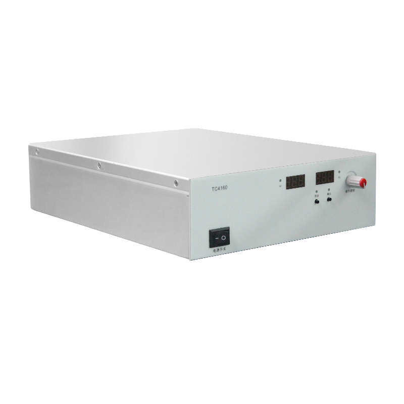
Charge Neutralization and Adsorption Force Control Mechanism of Bipolar High Voltage Power Supply for Electrostatic Chuck
Electrostatic chucks are essential components in semiconductor manufacturing equipment for holding wafers during processing. The chuck uses electrostatic forces to hold the wafer firmly while enabling precise temperature control. Bipolar high voltage power supplies provide both positive and negative voltages to enable charge neutralization and controlled adsorption forces. The implementation of these power supplies requires understanding of electrostatic chuck principles, wafer handling requirements, and charge management. The control mechanism must balance holding force with safe wafer release.
The electrical requirements for electrostatic chuck power supplies depend on the chuck design and wafer characteristics. Typical operating voltages range from hundreds to thousands of volts, with currents from microamps to milliamps depending on chuck capacitance and leakage. The power supply must provide both positive and negative voltages for charge neutralization while maintaining precise control of holding force. The load presented by the chuck varies with wafer size, backside conditions, and temperature, requiring the power supply to adapt to these variations.
Electrostatic chuck fundamentals rely on dielectric polarization. The chuck includes electrodes embedded in a dielectric material. When voltage is applied, the dielectric polarizes, creating an electrostatic attraction force between the chuck and wafer. The holding force depends on the applied voltage, dielectric properties, and chuck geometry. The power supply must provide the appropriate voltage to achieve the required holding force while enabling safe wafer release.
Bipolar operation enables charge neutralization. After processing, residual charge on the wafer or chuck can prevent clean release. Applying opposite polarity voltage neutralizes this residual charge, enabling easy wafer removal. The power supply must provide both positive and negative voltages with precise control. Charge neutralization is critical for preventing wafer damage during unloading.
Adsorption force control determines wafer holding stability. The holding force must be sufficient to prevent wafer movement during processing while allowing controlled release. The power supply must modulate the voltage to achieve the desired force profile. Force control may include ramp-up, steady-state, and ramp-down phases. Advanced control may implement adaptive force adjustment based on process conditions.
Dielectric properties affect chuck performance. The dielectric constant determines the capacitance and force generation capability. Dielectric strength limits the maximum applicable voltage. Surface properties affect charge retention and wafer release characteristics. The power supply must accommodate the specific dielectric material used in the chuck. Dielectric selection must balance performance, reliability, and cost.
Wafer backside conditions affect electrical contact. The wafer backside may have coatings or treatments that affect electrical characteristics. These coatings can affect charge transfer and holding force. The power supply must adapt to different backside conditions while maintaining consistent performance. Backside condition variations must be considered in chuck design and control strategy.
Temperature effects influence chuck performance. Dielectric properties change with temperature, affecting capacitance and force generation. Thermal expansion can affect chuck geometry and wafer contact. The power supply must compensate for temperature variations to maintain consistent holding force. Temperature compensation may be implemented in the control algorithm.
Leakage current management is important for stable operation. Leakage through the dielectric or across surfaces can reduce holding force and affect charge neutralization. The power supply must compensate for leakage to maintain the desired voltage and force. Leakage monitoring can provide diagnostic information about chuck condition. Leakage management is critical for long-term reliability.
Voltage ramp control affects wafer handling safety. Rapid voltage changes can cause wafer movement or damage. The power supply must control voltage ramp rates during both clamping and unclamping. Ramp control must balance speed with safety. Advanced systems may implement adaptive ramp rates based on process conditions.
Charge monitoring enables process optimization. The power supply can monitor charge accumulation and dissipation during operation. This information can be used to optimize clamping and unclamping sequences. Charge monitoring may also provide diagnostic information about chuck and wafer condition. Advanced monitoring may implement predictive algorithms for process improvement.
Safety considerations are paramount for wafer handling. The power supply must prevent accidental release during processing while ensuring reliable release when required. Safety interlocks and fault detection must be implemented. The system must protect wafers from electrostatic discharge damage. Safety design must balance protection requirements with operational efficiency.
Process integration affects control requirements. The electrostatic chuck must coordinate with other process subsystems such as temperature control, gas delivery, and vacuum systems. The power supply must integrate with the overall process control architecture. Integration considerations include timing, communication, and fault handling. The system design must optimize overall process performance.
Future semiconductor processes will demand more precise chuck control. As device geometries shrink, the requirements for wafer positioning and stability become more stringent. The power supply must provide improved force control, faster response, and better charge management. Advanced control techniques and sensor integration will be required. The continued evolution of electrostatic chuck technology will support the advancement of semiconductor manufacturing.