


Radiation Hardened Design of High Voltage Power Supply Based on Wide Bandgap Semiconductor Devices
High voltage power supplies operating in radiation environments such as space, nuclear facilities, and high-energy physics experiments face unique challenges from ionizing radiation. Radiation can cause degradation and failure of semiconductor devices through total ionizing dose effects, displacement damage, and single event phenomena. Wide bandgap semiconductor devices including silicon carbide and gallium nitride offer inherent advantages for radiation-hardened applications due to their superior material properties. The design of radiation-hardened high voltage power supplies using wide bandgap devices requires understanding of radiation effects, device selection, and circuit design techniques for radiation tolerance.
The electrical requirements for radiation-hardened high voltage power supplies depend on the specific application and radiation environment. Typical operating voltages range from hundreds to thousands of volts, with power levels from watts to kilowatts depending on the application. The power supply must provide stable output while operating in radiation fields that can cause gradual degradation and sudden upsets. The radiation environment may include gamma rays, protons, neutrons, and heavy ions, each with different effects on semiconductor devices. The power supply must maintain performance throughout the mission lifetime despite cumulative radiation exposure.
Total ionizing dose effects cause gradual degradation of semiconductor device characteristics. Ionizing radiation creates electron-hole pairs in insulating layers, particularly gate oxides in MOSFETs. The trapped charges shift threshold voltages, increase leakage currents, and reduce transconductance. Wide bandgap devices have thicker gate oxides or different gate structures that provide improved total ionizing dose tolerance compared to silicon devices. Silicon carbide MOSFETs generally show better total ionizing dose tolerance than silicon MOSFETs due to their thicker oxide layers. The power supply design must account for the expected total ionizing dose over the mission lifetime.
Displacement damage affects the bulk semiconductor material by displacing atoms from their lattice positions. These defects act as recombination centers, reducing carrier lifetime and mobility. In bipolar devices, displacement damage causes gain degradation and increased leakage. In unipolar devices such as MOSFETs, the effects are generally less severe but can still affect on-resistance and switching characteristics. Wide bandgap materials have higher displacement energy thresholds, making them more resistant to displacement damage. The power supply design must select devices with adequate displacement damage tolerance for the expected radiation environment.
Single event effects are caused by individual energetic particles striking sensitive device regions. Single event transients can cause temporary circuit upsets that may or may not be recoverable. Single event burnout and single event gate rupture can cause permanent device damage in power semiconductors. Wide bandgap devices have different single event susceptibility compared to silicon devices due to their different material properties and device structures. The power supply design must incorporate protection against single event effects including current limiting, voltage clamping, and fault detection.
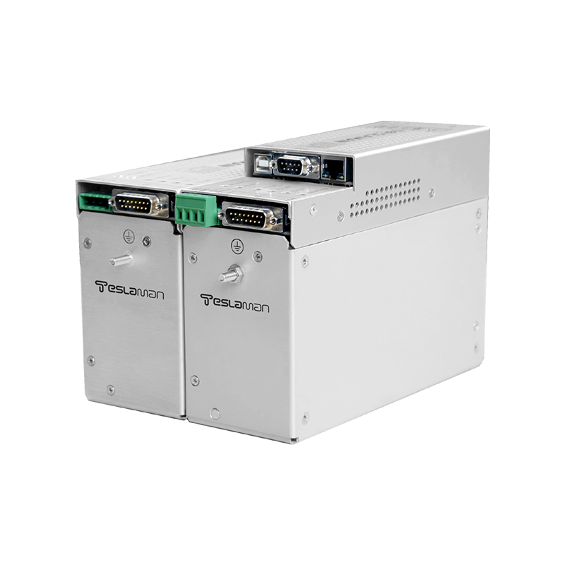
Silicon carbide devices offer significant advantages for radiation-hardened power supplies. Silicon carbide has a wide bandgap of 3.26 electron volts, compared to 1.12 electron volts for silicon. This wide bandgap provides higher breakdown voltage, higher operating temperature capability, and improved radiation tolerance. Silicon carbide MOSFETs and Schottky diodes are available with voltage ratings suitable for high voltage power supply applications. The material properties of silicon carbide make it inherently more resistant to many radiation effects compared to silicon.
Gallium nitride devices provide alternative options for radiation-hardened power conversion. Gallium nitride has a bandgap of 3.4 electron volts and offers high electron mobility and fast switching speed. Gallium nitride high electron mobility transistors are well-suited for high-frequency power conversion applications. The radiation tolerance of gallium nitride devices depends on the specific device structure and fabrication process. The lateral device structure commonly used for gallium nitride devices presents different radiation challenges compared to the vertical structures used for silicon carbide devices.
Circuit design techniques for radiation hardness complement device selection. Redundant circuits can provide continued operation if one circuit path is affected by radiation. Conservative derating of voltage and current ratings provides margin against radiation-induced degradation. Current limiting and voltage clamping protect against single event damage. Error detection and correction circuits mitigate the effects of radiation-induced digital upsets. The circuit design must implement multiple layers of protection to achieve the required radiation tolerance.
Insulation and dielectric materials in the high voltage sections must also be radiation tolerant. Radiation can degrade insulation materials, reducing dielectric strength and increasing leakage. Ceramic insulators generally have better radiation tolerance than organic insulation materials. The insulation design must account for radiation-induced degradation over the mission lifetime. Creepage and clearance distances must be increased to compensate for potential insulation degradation. Material selection for insulators, potting compounds, and circuit board materials must consider radiation tolerance.
Magnetic components present unique radiation hardness challenges. Transformer and inductor cores can be affected by radiation, causing changes in permeability and losses. Radiation can also affect the insulation on magnet wire, potentially causing short circuits. Amorphous and nanocrystalline core materials may have different radiation tolerance compared to conventional ferrite cores. The magnetic component design must account for potential radiation-induced changes in core characteristics. Potting and encapsulation can provide additional protection for magnetic components.
Testing and qualification for radiation hardness require specialized facilities and procedures. Total ionizing dose testing uses gamma ray sources such as cobalt-60 to expose devices to known radiation doses. Single event testing uses particle accelerators to bombard devices with heavy ions or protons. Displacement damage testing uses neutron sources or proton beams. The testing must be performed at representative operating conditions including temperature and bias. The test results provide the data needed to predict power supply performance in the radiation environment.
Design margin and derating practices are essential for radiation-hardened designs. Radiation effects introduce additional uncertainty in device characteristics and lifetime. Conservative derating of voltage, current, and temperature ratings provides margin against radiation-induced degradation. The design margin must account for both the initial device parameter spread and the expected radiation-induced drift. Design margin trades against performance, size, and cost, requiring careful optimization for the specific application.
Packaging and interconnect design affect radiation hardness. The device packaging must protect the semiconductor die from radiation while providing electrical and thermal connections. Some packaging materials can become activated by neutron radiation, creating additional radiation hazards. Wire bonds and solder joints can be affected by radiation-induced material changes. The packaging design must also consider outgassing in vacuum environments for space applications. The interconnect design must maintain reliability despite radiation-induced material degradation.
System-level radiation effects must be considered in addition to component-level effects. Radiation can cause charging of spacecraft structures, affecting the power supply grounding and reference potentials. Secondary radiation from shielding materials can create localized radiation hotspots. The system design must optimize shielding to reduce radiation exposure while managing weight and cost constraints. The power supply must be designed as part of the complete system radiation protection strategy.