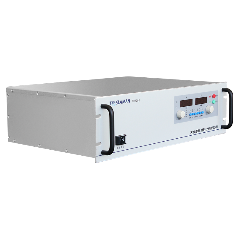
FPGA-Based Full Digital Phase Shift Control High Voltage Power Supply Feedback Loop Design
Digital control has become increasingly prevalent in power supply design due to advantages in flexibility, precision, and advanced control algorithms. Field programmable gate arrays offer high-speed parallel processing capability ideal for power supply control loops. Phase shift control is a technique used in resonant converters for efficient power conversion. The implementation of phase shift control in FPGA enables precise timing and adaptive control. Understanding the digital control design principles enables development of high-performance power supplies.
The electrical requirements for digitally controlled power supplies depend on the topology and application. The control loop must regulate output voltage or current with specified accuracy and response time. The phase shift control adjusts the timing between switching events to control power transfer. The digital controller must execute the control algorithm with sufficient speed and precision. The FPGA implementation must meet the real-time requirements of the power converter.
Phase shift control fundamentals involve timing adjustment between converter switches. In full-bridge converters, the phase shift between the two bridge legs controls the power transfer. Zero voltage switching can be maintained across the load range through proper phase shift control. The phase shift angle determines the effective duty cycle applied to the transformer. The control resolution affects the output regulation precision.
Digital control advantages include programmability and precision. Control parameters can be adjusted through software without hardware changes. Advanced algorithms can be implemented that would be impractical with analog circuits. The digital implementation provides immunity to component drift and temperature effects. The flexibility enables optimization for different operating conditions.
FPGA architecture provides parallel processing capability. Multiple operations can execute simultaneously rather than sequentially. This parallelism enables high-speed control loop execution. The FPGA can implement custom logic optimized for the specific application. The programmability enables field updates and algorithm refinement. The FPGA selection must balance capability, cost, and power consumption.
Feedback loop design in digital control follows similar principles to analog control. The error between reference and output drives the control action. Proportional, integral, and derivative terms can be implemented digitally. The sampling rate affects the achievable bandwidth. The quantization resolution affects the steady-state accuracy. The digital implementation must address these unique considerations.
Sampling and analog-to-digital conversion affect control performance. The sampling rate must be high enough to capture the relevant dynamics. The ADC resolution must be sufficient for the required precision. The sampling timing must be synchronized with the power stage switching. The sampling must not introduce aliasing or distortion. The ADC performance directly affects the control performance.
Digital pulse width modulation generates the gate drive signals. The resolution of the PWM affects the output precision. The PWM frequency must be appropriate for the power stage. The dead time between complementary switches must be precisely controlled. The FPGA can generate multiple PWM signals with precise timing relationships. The PWM generation must be reliable and glitch-free.
Phase shift implementation requires precise timing control. The phase relationship between bridge legs determines the power transfer. The timing resolution affects the phase shift precision. The phase shift must be adjustable across the required range. The timing must be maintained despite variations in operating conditions. The FPGA timers must have adequate resolution for the required precision.
Protection functions can be implemented in the FPGA. Overcurrent protection responds to fault conditions. Overvoltage protection prevents output damage. Over-temperature protection prevents thermal damage. The protection functions must respond quickly enough to prevent damage. The FPGA implementation enables fast protection response.
Communication interfaces enable parameter adjustment and monitoring. Serial interfaces connect to external controllers. Digital interfaces connect to system buses. The communication must be reliable and properly timed. The interface design must not interfere with the control loop execution. The communication protocols must be appropriate for the application.
Development tools support FPGA programming. Hardware description languages define the FPGA logic. Simulation tools verify the design before implementation. Debugging tools support development and troubleshooting. The development environment must support the required complexity. The development process must ensure reliable operation.
Testing and validation verify the control performance. Step response testing verifies transient performance. Frequency response testing verifies stability margins. Long-term testing verifies reliability. The testing must cover all operating conditions. The validation must demonstrate that the design meets requirements.
Applications of digital phase shift control include server power supplies, electric vehicle chargers, and industrial power systems. Each application has specific requirements for performance and features. The digital control design must support the specific application requirements.