Electromagnetic Compatibility and Layout Optimization of Integrated High Voltage Power Supply for Microwave Power Module
Microwave power modules represent a sophisticated integration of vacuum electron device technology with solid-state electronics, combining the high power and efficiency of traveling wave tubes or klystrons with the reliability and convenience of solid-state amplifiers. The high voltage power supply integrated within these modules must operate in close proximity to high-power microwave circuits, creating challenging electromagnetic compatibility requirements. Successful integration demands careful attention to layout optimization and EMC design principles to prevent interference that could degrade performance or cause malfunction.
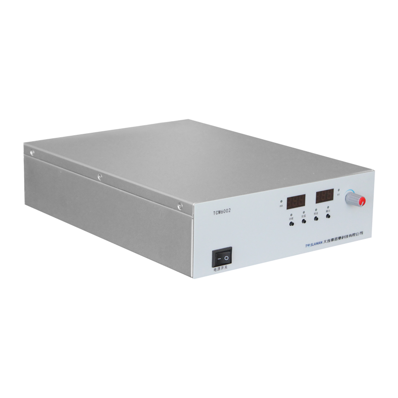
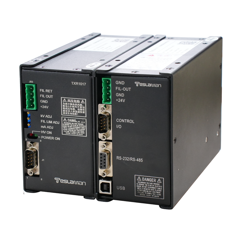
The architecture of a microwave power module typically includes several distinct functional blocks that must coexist within a compact enclosure. A solid-state driver amplifier boosts the input signal to a level suitable for driving the vacuum device. The vacuum electron device, whether a traveling wave tube, klystron, or crossed-field amplifier, provides the final power amplification to achieve the required output power. The high voltage power supply generates the multiple voltages needed for cathode, anode, grid, and collector electrodes. Control circuits regulate the power supply and monitor system health. All these components must operate together without mutual interference.
The high voltage power supply presents particular EMC challenges due to its inherent noise generation. Switching power converters, commonly used for their efficiency and compact size, generate conducted and radiated electromagnetic interference through the rapid switching of high currents and voltages. The switching frequency and its harmonics can extend into frequency ranges that overlap with the operating frequencies of the microwave circuits. Without proper mitigation, this interference can couple into sensitive receiver circuits or modulate the output signal, degrading system performance.
Shielding strategies form the first line of defense against electromagnetic interference. The power supply circuits can be enclosed within conductive enclosures that attenuate radiated emissions. The effectiveness of shielding depends on the conductivity and permeability of the shield material, the thickness relative to skin depth at the frequencies of concern, and the integrity of seams and apertures. Any openings in the shield, whether for ventilation, cable entry, or component access, must be designed to prevent leakage of electromagnetic energy. Gasketing materials and waveguide-beyond-cutoff apertures can maintain shielding effectiveness while accommodating necessary openings.
Filtering addresses conducted interference that would otherwise propagate through power and signal connections. Input filters prevent switching noise from the power supply from contaminating the prime power source. Output filters smooth the high voltage outputs and attenuate ripple and noise. Signal line filters prevent interference from entering or leaving through control and monitoring interfaces. The filter design must account for the impedance environment at both input and output ports, the frequency range of concern, and the current and voltage ratings of the application.
Grounding design profoundly influences EMC performance. A well-designed grounding system provides low-impedance return paths for signal and power currents while preventing ground loops that could couple interference. In integrated microwave power modules, the grounding strategy must accommodate the different requirements of high voltage power circuits, low-level signal circuits, and high-power microwave circuits. Separation of ground domains with controlled interconnection points can prevent noise coupling while maintaining safety and functionality.
Layout optimization involves the physical arrangement of components and interconnects to minimize interference coupling. Sensitive circuits should be physically separated from noise-generating circuits where possible. The routing of conductors should minimize loop areas that could act as antennas for radiated interference. High di/dt paths should be kept short to reduce magnetic field coupling. High dv/dt nodes should have minimal exposed surface area to reduce electric field coupling. These principles apply both to the internal layout of the power supply and to its placement within the overall module.
The thermal design of the power supply interacts with EMC design in several ways. Shielding enclosures can impede heat dissipation, requiring thermal management solutions that maintain EMC integrity. Heat sinks may need to be electrically isolated or connected to appropriate ground points. Cooling apertures must be designed to block electromagnetic leakage while allowing adequate airflow. The choice between conduction, convection, and liquid cooling affects the mechanical design and may influence EMC solutions.
Component selection influences both EMC performance and reliability. Components with low parasitic inductance and capacitance help to minimize high-frequency noise generation. Capacitors with low equivalent series resistance and inductance provide effective high-frequency filtering. Ferrite materials can be selected for optimal impedance at the frequencies of concern. The voltage and current ratings of components must provide adequate margin for reliable operation under all expected conditions.
Testing and verification ensure that the integrated system meets its EMC requirements. Conducted emission measurements verify that input and output noise levels are within specifications. Radiated emission measurements confirm that shielding is effective. Susceptibility testing verifies that the system can operate correctly in the presence of external electromagnetic fields. These tests should be performed on the fully integrated module to capture any interactions that might not be apparent from testing subsystems in isolation.