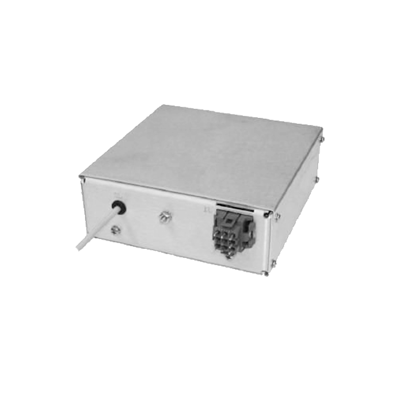
Effect of Dielectric Layer Thickness Uniformity on Holding Force of Electrostatic Chuck High Voltage Power Supply
Electrostatic chucks have become indispensable wafer handling devices in semiconductor manufacturing equipment, providing secure and uniform clamping without the mechanical contact and contamination risks associated with conventional clamp rings. The holding force generated by an electrostatic chuck depends critically on the electric field distribution between the chuck electrodes and the wafer surface, which is determined by the applied voltage and the dielectric layer properties. The thickness uniformity of this dielectric layer emerges as a key manufacturing parameter that directly influences the uniformity and magnitude of the holding force across the wafer surface. Understanding this relationship enables optimization of chuck design and manufacturing processes for reliable wafer handling in advanced semiconductor fabrication.
The electrostatic chuck operates on the principle of electrostatic attraction between charged electrodes and a conductive or semiconductive workpiece. The chuck structure typically consists of a metal base plate, one or more electrode patterns, and a dielectric layer covering the electrodes. When high voltage is applied to the electrodes, an electric field develops across the dielectric layer, inducing image charges in the wafer and creating an attractive force that holds the wafer against the chuck surface. The holding force per unit area is proportional to the square of the electric field strength and the permittivity of the dielectric material.
The electric field strength in the dielectric layer is inversely proportional to the layer thickness for a given applied voltage. Thinner dielectric regions experience higher electric fields and generate stronger local holding forces, while thicker regions produce weaker forces. This thickness dependence means that any nonuniformity in the dielectric layer translates directly into nonuniformity in the holding force distribution across the wafer. Localized regions of thin dielectric create force concentrations that may cause wafer distortion or damage, while thick regions may provide insufficient holding force to prevent wafer movement during processing.
The relationship between thickness variation and force nonuniformity can be quantified through analysis of the electric field distribution. For a dielectric layer with thickness varying around a nominal value, the local electric field varies inversely with the local thickness. The holding force, being proportional to the square of the field, varies with the inverse square of the thickness. A thickness variation of a few percent can therefore produce force variations of roughly twice that percentage, amplifying the effect of manufacturing tolerances on chuck performance.
Manufacturing processes for electrostatic chuck dielectric layers must achieve exceptional thickness uniformity to meet the demanding requirements of semiconductor wafer handling. Plasma sprayed ceramic coatings, commonly used for their thermal and electrical properties, can exhibit thickness variations from coating process nonuniformities, spray pattern effects, and substrate preparation variations. Polishing or grinding processes applied after coating can improve uniformity but introduce their own variations from tool wear, process control limitations, and material removal nonuniformity. Alternative dielectric deposition methods including physical vapor deposition and chemical vapor deposition offer potentially better uniformity control but may have limitations on achievable thickness or material properties.
The dielectric material properties also affect the holding force and its uniformity. The dielectric constant determines the capacitance per unit area and influences the charge induced in the wafer for a given voltage. Variations in dielectric constant across the chuck surface, arising from material composition variations or porosity differences, contribute to force nonuniformity in addition to thickness effects. The dielectric strength limits the maximum electric field that can be applied without breakdown, constraining the maximum holding force achievable with a given dielectric thickness.
Wafer contact conditions at the chuck surface influence the effective holding force and its sensitivity to dielectric nonuniformity. Real wafer surfaces are not perfectly flat, and microscopic gaps between the wafer and chuck surface reduce the effective holding force compared to ideal contact conditions. Backside particles or contamination on either the wafer or chuck surface create local separations that further reduce the local holding force. The dielectric thickness uniformity interacts with these contact effects, as variations in surface height from dielectric thickness differences can create or exacerbate contact gaps.
Temperature effects during processing introduce additional considerations for dielectric thickness and holding force. Thermal expansion of the dielectric material changes the layer thickness with temperature, potentially modifying the thickness uniformity if the thermal expansion is not uniform across the chuck surface. The dielectric constant may also be temperature dependent, affecting the holding force through both thickness and permittivity changes. High temperature processing steps require dielectric materials that maintain their electrical and mechanical properties throughout the operating temperature range.
The high voltage power supply characteristics interact with the dielectric properties to determine the actual holding force. The applied voltage must be selected considering the dielectric thickness and strength to achieve the required holding force while maintaining adequate margin from breakdown. Voltage stability affects the consistency of the holding force over time, with ripple or drift causing corresponding force variations. The power supply current capability must be sufficient to charge the chuck capacitance quickly during wafer clamping operations.
Measurement and characterization of dielectric thickness uniformity employs various techniques including ultrasonic thickness gauging, capacitive mapping, and optical interferometry. Ultrasonic methods measure the time of flight of acoustic pulses through the dielectric layer, converting to thickness using the acoustic velocity in the material. Capacitive mapping measures the local capacitance between a probe electrode and the chuck electrode, relating to the local dielectric thickness. Optical methods can provide high resolution thickness maps but require appropriate surface reflectivity and may be affected by dielectric transparency.
Process control for dielectric thickness during manufacturing relies on in process measurements and statistical process control methods. Target thickness values and tolerance limits are established based on the holding force requirements and the sensitivity analysis relating thickness variations to force nonuniformity. Regular monitoring of thickness uniformity metrics enables detection of process drift and implementation of corrective actions to maintain chuck quality.