Precision Control and Process Optimization of High Voltage Transfer Printing Power Supply for Flexible Electronics Manufacturing
Flexible electronics manufacturing produces electronic devices on flexible substrates such as polymer films, paper, or textile materials. Transfer printing techniques enable patterning of electronic materials on flexible substrates by transferring patterns from a donor substrate. High voltage electrostatic transfer printing uses electric fields to assist the transfer process, providing precise control of the transfer location and timing. The high voltage power supply for transfer printing must provide precise, controlled voltage that enables accurate pattern transfer.
Transfer printing processes transfer material patterns from a donor substrate to a receiver substrate. The donor substrate contains the patterned material, often created by conventional fabrication techniques on a rigid substrate. The receiver substrate receives the transferred pattern, building the flexible electronic device. The transfer can use various mechanisms including adhesive transfer, thermal release, and electrostatic transfer.
Electrostatic transfer printing uses electric fields to drive the transfer of material from donor to receiver. The donor and receiver substrates are positioned with the pattern facing the receiver. Voltage applied between the substrates creates an electric field that exerts electrostatic force on the patterned material. The force assists the transfer, enabling selective transfer of specific pattern elements.
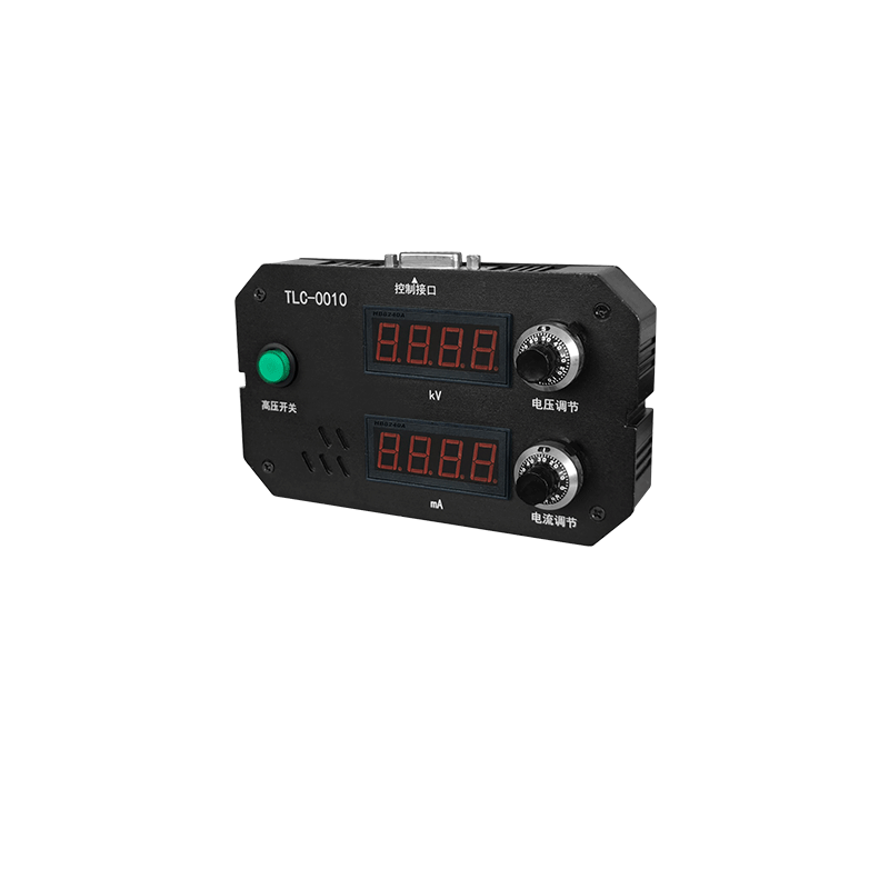
The high voltage power supply provides the voltage for electrostatic transfer. The voltage determines the electrostatic force, with higher voltages producing stronger forces. The voltage must be sufficient to overcome the adhesion between the pattern and the donor substrate, enabling transfer to the receiver. The voltage must not be excessive, which could cause uncontrolled transfer or damage to the materials.
Voltage precision affects the transfer accuracy and selectivity. Precise voltage control enables transfer of specific pattern elements while leaving others on the donor. The voltage threshold for transfer depends on the material properties and the adhesion strength. Operating near the threshold enables selective transfer, with elements transferring only when voltage exceeds their individual thresholds.
Voltage timing affects the transfer sequence. The voltage application timing determines when transfer occurs relative to substrate positioning and other process steps. Rapid voltage application enables quick transfer once substrates are aligned. Controlled voltage rise enables gradual transfer that may improve transfer quality. The timing must coordinate with the mechanical motion of the transfer system.
Spatial control of the electric field enables transfer at specific locations. Patterned electrodes or localized voltage application create electric fields at specific regions, enabling transfer of specific pattern elements. The spatial control enables sequential transfer of different elements to build complex patterns. The electrode design must provide the required spatial resolution for the pattern elements.
Multi layer transfer builds complex devices through sequential transfer of multiple pattern layers. Each layer transfers from a donor substrate to the receiver, building up the device structure. The voltage parameters may differ for different layers, depending on the material properties and the transfer requirements. The power supply must enable different voltage settings for different transfer steps.
Material properties affect the transfer voltage requirements. Different materials have different electrostatic properties and different adhesion to substrates. Materials with higher chargeability may transfer at lower voltage. Materials with stronger adhesion may require higher voltage. The voltage optimization must account for the specific materials being transferred.
Substrate properties affect the electric field distribution and the transfer behavior. The substrate dielectric properties affect the field penetration. The substrate conductivity affects the charge distribution. The substrate surface properties affect the adhesion. The voltage parameters must be optimized for the specific substrate combination.
Process optimization determines the voltage parameters that achieve optimal transfer quality. The optimization considers transfer completeness, transfer accuracy, and material integrity. Complete transfer requires sufficient voltage to transfer all intended elements. Accurate transfer requires precise voltage to transfer elements to the correct locations. Material integrity requires appropriate voltage to avoid damage during transfer.
Quality assessment of transferred patterns measures the transfer success. Visual inspection reveals the transferred pattern appearance. Electrical testing measures the functionality of transferred electronic elements. Microscopic examination reveals the transfer morphology and any defects. The quality assessment guides the process optimization.
Production implementation of electrostatic transfer printing requires integration with manufacturing systems. The high voltage power supply must interface with the transfer printing equipment, receiving control signals and providing the required voltage. The integration must maintain the precision and timing requirements in the production environment. The power supply reliability must support production throughput requirements.