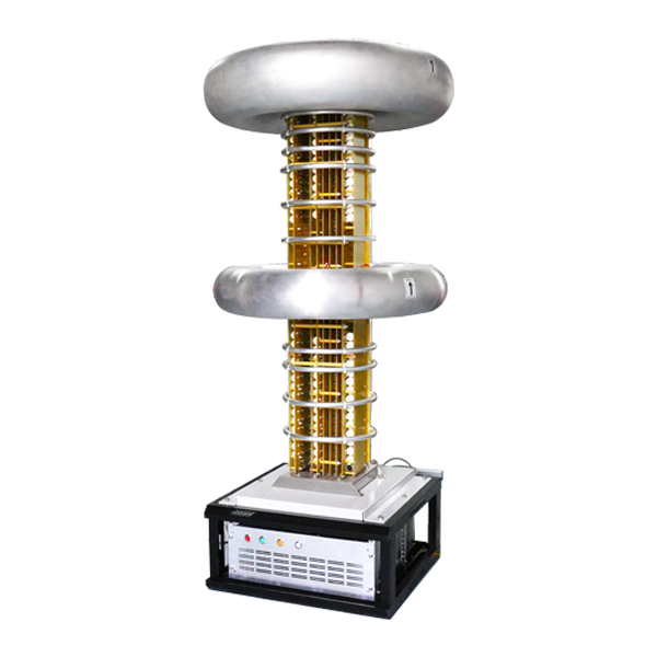
Back EMF Protection and Energy Recovery Circuit of High Voltage Power Supply with Inductive Load
High voltage power supplies driving inductive loads face unique challenges related to the energy stored in the magnetic field of the inductance. When current flow through an inductor is interrupted, the magnetic field collapses, inducing a voltage that opposes the change in current. This back electromotive force can reach extremely high voltages that pose risks to power supply components and connected equipment. Effective protection circuits and energy recovery mechanisms are essential for reliable operation of high voltage systems with inductive loads.
The fundamental physics of inductive kickback derives from Faradays law of electromagnetic induction. The voltage induced across an inductor is proportional to the rate of change of current and the inductance value. When current is rapidly interrupted, the rate of change can be very large, resulting in correspondingly large induced voltages. In high voltage applications with substantial inductance, these induced voltages can easily exceed the ratings of semiconductor devices and insulation systems.
Protection against back EMF requires providing an alternative current path for the inductor current when the primary current path is interrupted. This alternative path allows the inductor current to decay gradually rather than being forced to instantaneously stop, limiting the magnitude of the induced voltage. Various circuit topologies provide this current path with different characteristics in terms of response time, energy dissipation, and complexity.
Freewheeling diodes represent the simplest form of back EMF protection. A diode connected in reverse polarity across the inductive load provides a current path when the driving voltage is removed. The inductor current circulates through the diode, gradually decaying as energy is dissipated in the diode forward voltage drop and the inductor resistance. This approach is simple and reliable but dissipates the stored energy as heat rather than recovering it.
Snubber circuits provide more sophisticated back EMF protection by combining capacitors with resistors and sometimes diodes. The capacitor absorbs energy from the inductor during turn-off, limiting the voltage rise rate. The resistor dissipates the absorbed energy during subsequent cycles. Snubber circuits can be optimized for specific applications by selecting component values that balance protection effectiveness against power dissipation.
Metal oxide varistors offer another approach to back EMF protection by providing voltage-dependent resistance. Under normal operating voltages, the varistor presents high impedance and draws negligible current. When the voltage exceeds the varistor threshold, the impedance drops dramatically, conducting current and limiting the voltage excursion. Varistors can absorb substantial energy pulses and provide effective protection against occasional voltage transients.
Energy recovery circuits go beyond simple protection by capturing the energy stored in the inductor and returning it to a useful form. This approach improves overall system efficiency and reduces thermal management requirements. Various energy recovery topologies have been developed for different application requirements and power levels.
Flyback converter topologies inherently provide energy recovery by transferring the inductor energy to an output capacitor through a diode during the off-time of the switching transistor. This approach is commonly used in switched-mode power supplies and can be adapted for high voltage applications with inductive loads. The recovered energy can be returned to the input supply, stored in a capacitor for later use, or dissipated in a controlled manner.
Active clamp circuits use auxiliary switches and capacitors to capture inductor energy and either return it to the supply or transfer it to a useful load. These circuits can achieve high efficiency recovery but require additional complexity in control and component count. The timing of the auxiliary switch must be precisely coordinated with the main switch to achieve effective clamping and energy recovery.
Regenerative snubber circuits combine the voltage limiting function of passive snubbers with energy recovery capability. These circuits use inductors and capacitors to transfer energy from the snubber capacitor back to the supply or load. The additional components increase complexity and cost but can significantly improve efficiency in high power applications where snubber losses would otherwise be substantial.
The design of back EMF protection circuits must consider the specific characteristics of the inductive load and the power supply. The inductance value determines the amount of energy stored and the magnitude of potential voltage transients. The load resistance affects the natural decay time constant of the inductor current. The switching frequency and duty cycle determine the average power that must be handled by the protection circuit.
High voltage insulation coordination requires careful attention to the voltage transients generated by inductive loads. The peak voltage during turn-off must be limited to values below the insulation ratings of transformers, cables, and other components. Voltage margins must account for the possibility of multiple transients occurring in quick succession, which can cause cumulative stress on insulation systems.
Semiconductor device selection for back EMF protection circuits must account for the voltage and current stresses during transient events. Devices must have adequate voltage ratings to withstand the peak voltages that can occur during worst-case conditions. Current ratings must handle the peak currents that flow during energy dissipation or recovery. Fast switching devices minimize switching losses but may generate higher frequency transients that require additional filtering.
Thermal management in protection circuits depends on the energy that must be dissipated and the frequency of transient events. Continuous operation with frequent switching may require substantial heat sinking for protection components. Energy recovery circuits reduce thermal management requirements by returning energy to the system rather than dissipating it as heat.
Testing and verification of back EMF protection circuits require specialized equipment and procedures. Inductive loads must be switched under various operating conditions to verify that voltage transients remain within acceptable limits. Energy recovery efficiency can be measured by comparing input and output energy over complete operating cycles. Long-term reliability testing verifies that protection circuits can withstand repeated transient events without degradation.
Fault conditions such as short circuits or open circuits in the load present additional challenges for protection circuits. Short circuits can cause excessive current flow that stresses both the power supply and protection components. Open circuits eliminate the normal current path and may cause protection circuits to handle the full stored energy of the inductor. Protection circuits must be designed to handle these fault conditions safely.
Electromagnetic interference generated by inductive switching can affect nearby electronic equipment and may not meet regulatory requirements without additional mitigation. The rapid current and voltage changes during switching generate broadband electromagnetic energy. Shielding, filtering, and careful layout reduce both conducted and radiated interference. Snubber circuits can also help reduce electromagnetic interference by slowing voltage transitions.
Control system integration for back EMF protection circuits requires coordination between the protection function and the normal power supply operation. Soft start circuits limit inrush current and reduce stress on protection components during startup. Sequencing circuits ensure that protection circuits are active before load current is applied. Fault detection circuits identify abnormal conditions and initiate appropriate protective actions.
Continued advancement in power electronics technology enables improved back EMF protection and energy recovery circuits. Higher voltage semiconductor devices expand the range of applications that can be served. Faster switching devices enable more precise control of transient events. Advanced control algorithms optimize the balance between protection effectiveness and energy recovery efficiency. These developments continue to improve the reliability and efficiency of high voltage systems with inductive loads.