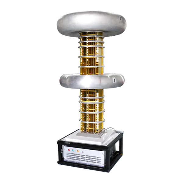
Electron Multiplier High Voltage Power Supply Channel Electron Multiplication Technology Integrated Application
Channel electron multipliers represent specialized vacuum tube devices that amplify weak electron signals through secondary electron emission in a continuous dynode structure. The integrated application of channel electron multiplication technology with high voltage power supply systems enables detection of single particles and photons across scientific research, analytical instrumentation, and industrial monitoring applications. Understanding the interaction between multiplier characteristics and power supply parameters enables optimization of detection systems for specific application requirements, directly affecting measurement sensitivity and accuracy.
The channel electron multiplier structure consists of a curved or helical channel with a conductive coating on the inner surface. Electrons entering the input end of the channel accelerate through the applied electric field, striking the channel wall and releasing secondary electrons. These secondary electrons in turn accelerate and strike the wall, producing additional electrons. The multiplication process continues along the channel length, producing gains of millions at typical operating voltages. The curved geometry prevents positive ions generated in the multiplication process from traveling back to the input, eliminating ion feedback that would cause spurious pulses and gain instability. The channel geometry must be optimized for specific application requirements including gain, timing resolution, and count rate capability.
The relationship between applied voltage and gain follows an approximately exponential function over the normal operating range. Small voltage changes produce large gain changes, making precise voltage control essential for stable gain. The gain-voltage coefficient varies with channel geometry, surface treatment, and operating history, but typical values range from 10 to 30 percent gain change per percent voltage change. Power supply stability directly determines gain stability, with requirements often specified in parts per thousand or better for precision applications. The power supply must maintain this stability over time and temperature variations while supplying the bias current that flows through the multiplier channel. Gain calibration procedures must account for the nonlinear gain-voltage relationship.
The high voltage power supply architecture for channel electron multiplier operation typically follows one of several approaches depending on application requirements. Simple resistive biasing uses a voltage divider to distribute voltage along the channel, with the supply voltage applied between input and output. This approach requires minimal circuitry but provides limited control over the internal field distribution. Active biasing using multiple regulated supplies enables optimization of the field profile along the channel, potentially improving gain characteristics and dynamic range. The choice between approaches depends on the performance requirements and acceptable complexity. Field profile optimization can significantly improve detector performance for demanding applications.
Pulse counting applications represent the most common use of channel electron multipliers in scientific instrumentation. Single particle or photon detection requires sufficient gain to produce output pulses exceeding the noise floor of the subsequent electronics. Power supply noise can couple into the detection chain, producing baseline fluctuations that degrade pulse height resolution and detection sensitivity. Grounding and shielding practices become critical for achieving the best possible signal-to-noise ratio. The power supply must provide clean, stable high voltage while introducing minimal interference into the sensitive detection electronics. Noise characterization must include both conducted and radiated interference effects.
Count rate capability of channel electron multipliers depends on both the device characteristics and the power supply current capability. At high count rates, the charge extracted per pulse multiplied by the pulse rate determines the average output current. This current cannot exceed the bias current through the channel without causing gain reduction due to voltage drop across the channel resistance. The power supply must provide adequate bias current for the expected count rate while maintaining voltage accuracy. Pulse pile-up at high count rates can also cause gain depression, limiting count rate performance. Count rate characterization must cover the full expected operating range.
Gain saturation characteristics determine the useful dynamic range of the detector. At high output currents, the multiplication process becomes self-limiting as space charge effects reduce the electron energy and secondary emission yield. The gain begins to decrease as the output current approaches the bias current. Power supply design can influence saturation behavior through control of the bias current and voltage distribution. Higher bias currents provide higher linear output current capability but also increase power dissipation and may affect multiplier lifetime. Saturation characterization enables prediction of dynamic range limitations.
Timing characteristics of channel electron multipliers depend partly on power supply parameters. The transit time of electrons through the channel and its statistical variation determine the time resolution of the detector. While the fundamental transit time depends primarily on the channel geometry and applied voltage, power supply ripple and noise can introduce timing jitter that degrades resolution. Stable, low-noise power supplies help optimize timing performance in applications such as time-of-flight mass spectrometry or coincident detection experiments. Timing resolution characterization must include power supply noise effects.
Environmental factors affecting channel electron multiplier performance include temperature, pressure, and radiation exposure. The multiplier gain typically varies with temperature due to temperature coefficients in the secondary emission surfaces and resistive coating. Temperature-controlled environments or compensation circuits can mitigate these effects. Exposure to atmospheric pressure, even briefly, can contaminate the multiplier surfaces and degrade performance. The power supply system may include interlocks that prevent high voltage application when vacuum conditions are inadequate, protecting the multiplier from damage. Environmental qualification testing must verify performance under expected operating conditions.
Multi-channel electron multiplier arrays enable position-sensitive detection by providing independent outputs from multiple multiplier elements. Each channel requires independent gain control or at least uniform voltage distribution across the array. Power supply systems for multi-channel detectors must provide multiple outputs with matched characteristics, or distribution networks that ensure uniform voltage despite component variations. Temperature matching between channels may also be required for uniform gain across the array. Array calibration must account for channel-to-channel variations.
Aging and lifetime considerations influence power supply operating parameters and monitoring strategies. Channel electron multipliers exhibit gradual gain loss with accumulated charge extraction, eventually requiring replacement. Operating at lower gain extends lifetime but may compromise detection efficiency. Power supply monitoring of bias current trends can provide early warning of approaching end of life, enabling scheduled replacement before failure. The power supply voltage adjustment range must accommodate the voltage increase needed to maintain constant gain as the multiplier ages. Lifetime prediction models enable optimization of replacement scheduling.
Integration of the high voltage power supply with detector electronics presents packaging and noise management challenges. Proximity of high voltage circuits to sensitive amplifiers requires careful attention to electromagnetic compatibility. Shielding and physical separation help prevent high voltage noise from coupling into signal paths. Grounding strategies must account for both safety requirements and signal integrity requirements. Modular designs that separate high voltage generation from regulation and monitoring can simplify integration while providing flexibility for different detector configurations.