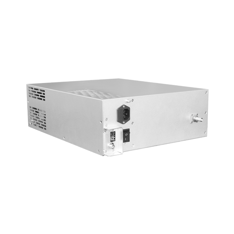
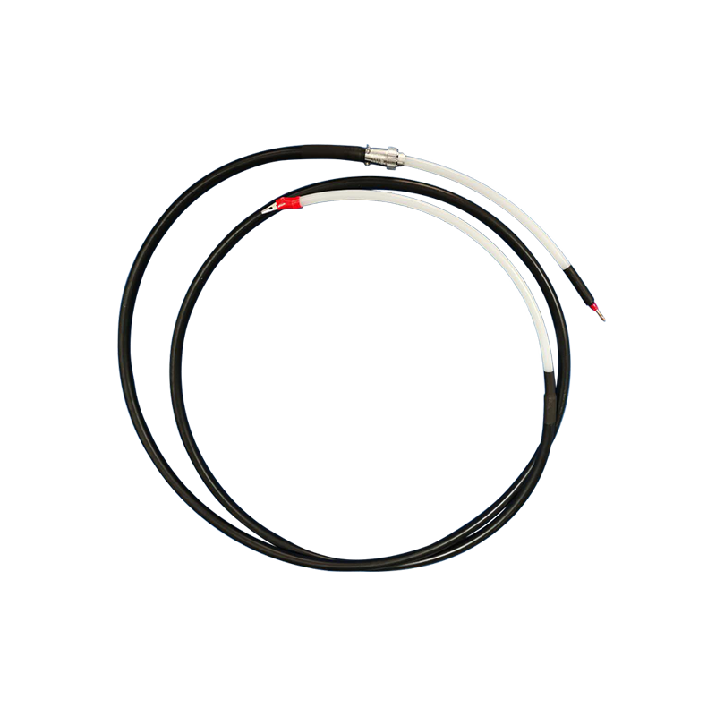
Ion Beam System High Voltage Power Supply Beam Stability in Ion Implanter
Ion implanters represent a critical process tool in semiconductor manufacturing, enabling the precise modification of electrical properties in silicon substrates through controlled ion bombardment. The performance of ion implanters is fundamentally dependent on the stability and precision of the ion beam, which is directly governed by the high voltage power supply. The power supply provides the accelerating potential that determines ion energy and controls the beam optics that shape and direct the ion beam toward the wafer. For advanced technology nodes, the beam stability requirements are extremely stringent, with energy spread specifications below 0.1 percent and beam angle control measured in milliradians. Meeting these requirements demands sophisticated power supply design that addresses multiple sources of beam instability.
The ion implanter power supply typically operates in the voltage range of 10 kilovolts to 300 kilovolts, depending on the required ion energy for specific implantation processes. Lower voltages in the 10 to 50 kilovolt range are used for shallow junction formation in advanced logic devices, while higher voltages up to 300 kilovolts are used for deep well implantation and backside processing. The power supply must deliver these voltages with exceptional stability, as any fluctuation in the accelerating voltage directly translates to corresponding variations in ion energy. The energy distribution of implanted ions determines the depth profile of the doped region, and even minute voltage variations can cause unacceptable broadening of the implantation profile. Closed-loop voltage regulation with a bandwidth of several kilohertz is employed to maintain output voltage within 0.05 percent of the target value. The regulation system uses a high-precision voltage divider with temperature-stable resistors and a high-resolution analog-to-digital converter for feedback measurement.
The power supply architecture for ion implanters incorporates multiple stages of voltage conversion and filtering. A three-phase rectifier produces a stable DC bus voltage that feeds into a high frequency inverter. The inverter output drives a step-up transformer with a toroidal core design to minimize leakage inductance and maximize coupling efficiency. The transformer output is rectified and filtered through a multi-stage LC filter network that achieves attenuation of switching harmonics by more than 80 decibels. An additional active filter stage provides final ripple suppression to levels below 0.005 percent, ensuring the accelerating voltage is essentially pure DC with negligible AC components. The entire high voltage section is housed in a sealed metal enclosure with controlled atmosphere to prevent corona discharge and arcing at high voltage levels.
Beam position and angle stability are influenced not only by voltage regulation but also by the mechanical and electrical design of the beam line components. The power supply must provide a low-noise environment for the beam steering and focusing electrodes. Any voltage ripple or noise on the deflection electrode supplies causes corresponding beam jitter, which degrades implantation uniformity across the wafer. The power supply incorporates separate low-noise output channels for beam steering and focusing circuits, with dedicated filtering and shielding for each channel. The output impedance of these channels is kept very low to prevent coupling of noise from the main acceleration circuit into the beam control circuits. This separation of electrical domains is essential for maintaining the required beam stability. The beam steering electrodes require ultra-stable voltage supplies with noise floors below one microvolt to ensure beam positioning accuracy at the sub-micrometer level.
Long-term reliability and maintainability are critical considerations for ion implanter power supplies used in high-volume manufacturing. The power supply design incorporates modular construction with easily replaceable sub-assemblies such as inverter modules, filter capacitors, and control boards. Advanced diagnostic systems monitor the health of critical components including transformer temperature, capacitor leakage current, and semiconductor device parameters. This data is analyzed by a predictive maintenance algorithm that identifies potential failures before they occur, allowing scheduled replacement during planned downtime. The power supply also includes built-in calibration routines that verify voltage accuracy and compensate for component drift over time. These features ensure that the ion implanter maintains its beam stability specifications throughout its operational life, supporting the demanding requirements of advanced semiconductor manufacturing. The modular design also allows for field upgrades of voltage ratings or control capabilities, extending the useful life of the power supply beyond its original design expectations.
The interaction between the high voltage power supply and the ion beam diagnostics system represents a critical feedback loop for maintaining implantation quality. Beam position monitors and energy analyzers provide real-time data on beam characteristics, which is processed by the implanter control system to adjust the power supply output. This feedback allows compensation for drift in beam line components and changes in ion source performance, maintaining the required beam stability throughout extended implantation campaigns. The power supply control system also coordinates with the wafer scanning system to adjust beam parameters during different phases of the implantation process, such as ramping up voltage for deep well regions or ramping down for shallow junctions. The synchronization of these adjustments with the wafer position ensures uniform doping across the entire wafer surface.
The electromagnetic compatibility of the ion implanter power supply is a critical design consideration due to the sensitive nature of the implanted device structures. The power supply generates electromagnetic noise through its switching operations and voltage transitions, which could potentially interfere with other process equipment or affect the electrical properties of the substrate being processed. Comprehensive shielding enclosures, filtered power connections, and controlled impedance grounding minimize electromagnetic emission. The power supply also incorporates gradient shielding layers that provide progressive attenuation of noise at different frequencies, ensuring that even high-frequency switching harmonics are effectively suppressed. These EMC measures are verified through standardized testing procedures to ensure compliance with semiconductor facility electromagnetic compatibility requirements.
The safety design of ion implanter power supplies addresses the hazards of high voltage operation and ion beam exposure. Multiple independent interlock systems prevent operation when any safety-critical condition is not met, including access panel security, beam line vacuum integrity, and radiation shielding status. The power supply incorporates controlled discharge paths that safely dissipate residual high voltage within milliseconds of shutdown, preventing electrical hazards during maintenance. The ion beam radiation is managed through comprehensive shielding that attenuates radiation levels to below regulatory limits at all accessible points. The power supply also includes emergency shutdown capabilities that can be triggered from multiple locations, providing rapid response to any unsafe condition. These safety features ensure that the ion implanter power supply meets the stringent safety requirements of semiconductor manufacturing facilities.